
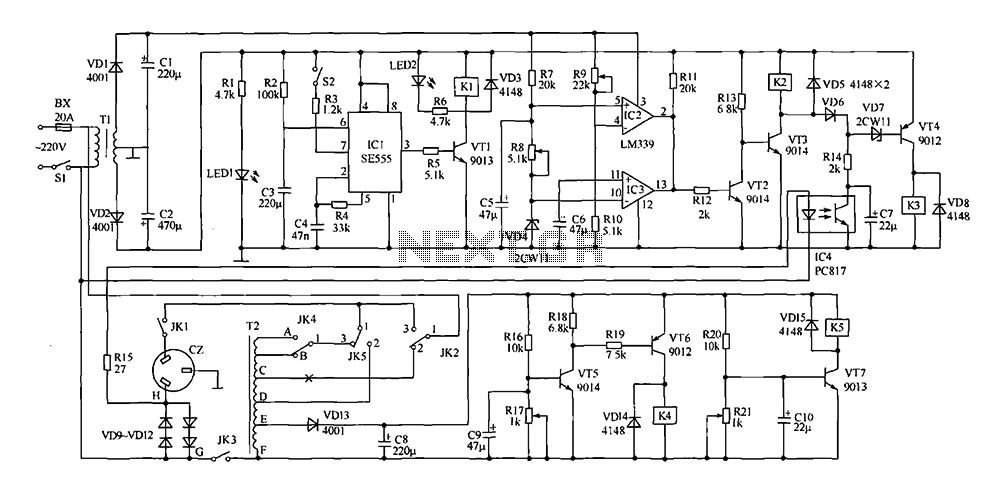
High-Low voltage cut-off with delay and alarm with circuit diagram

The high and low voltage cut-off circuit is designed to protect electrical devices from damage caused by excessive voltage or insufficient voltage levels. This circuit operates by monitoring the input voltage and triggering a cut-off mechanism when the voltage exceeds or drops below predetermined thresholds. The inclusion of a delay feature ensures that transient voltage spikes do not inadvertently activate the cut-off, allowing the system to stabilize before making a decision. Additionally, an alarm system is integrated to alert users when the voltage levels are outside the acceptable range.
The circuit typically consists of a voltage sensing circuit, which can be implemented using operational amplifiers or comparators. These components continuously monitor the input voltage and compare it against reference voltage levels set by resistive voltage dividers. When the input voltage exceeds the upper threshold or falls below the lower threshold, the comparator output changes state.
A delay mechanism is often implemented using an RC (resistor-capacitor) network, which provides a time delay before the cut-off action is initiated. This delay prevents nuisance tripping due to brief voltage fluctuations. The output of the comparator can be connected to a relay or a MOSFET, which acts as the cut-off switch to disconnect the load from the power source.
For the alarm function, a simple buzzer or LED indicator can be employed. When the voltage is outside the specified range, the alarm circuit can be activated, providing a visual or audible indication to the user. The alarm system can be designed to remain active until the user manually resets it, ensuring that the user is aware of the voltage issue.
Overall, this circuit is essential in applications where voltage stability is critical, such as in power supplies for sensitive electronic equipment, ensuring both protection and user awareness of potential electrical issues.The high and low voltage cut-off with delay and alarm circuit with circuit diagram is explained in this post.. 🔗 External reference
Related Circuits
This document presents a power-saving voltage regulator circuit. In addition to its general function as a delay regulator, the circuit features: (1) an automatic voltage regulation capability for mains voltage within a range of 220V ±10%, allowing direct power...
The construction is nearly complete, and a circuit diagram has been created. The design has been finalized and documented on paper. The circuit diagram represents a critical stage in the development of an electronic project, serving as a blueprint for...
Rosemary's original test circuit is shown in the article she tried to have published in a refereed scientific journal, but the submission was always rejected. In the last 5 months, I have had extensive email correspondence, and numerous telephone...
This circuit consists of two main components: a battery charger that provides a fixed output voltage of 5V DC, and a regulated power supply that allows for an adjustable output voltage ranging from 2 to 9 volts. The circuit design...
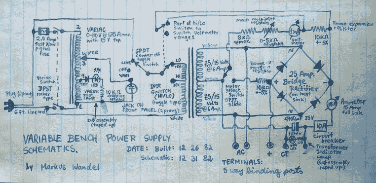
This power supply is able to deliver adjustable center-tapped DC from 0 to about 30 volts, as well as AC directly from the Variac and from the main transformer before the rectifier. What's primitive by today's standard is that...
The circuit incorporates components Q, C, and ZD, which are responsible for the bias and buffer stages. Its primary objective is to ensure stable MOSFET gate operation and provide an offset voltage through a voltage buffer amplifier stage with...