
Simple Power Supply Suits VoIP/PoE Applications

The power supply circuit is designed to efficiently support PoE and VoIP applications, ensuring that powered devices can reliably receive power through Ethernet cables. The inclusion of discovery and classification functionalities is crucial for compliance with PoE standards, allowing devices to negotiate power requirements seamlessly. The DP423G IC serves as the heart of the converter, facilitating high-frequency operation that is essential for compact power supply designs. The use of a flyback topology enables isolation between the input and output, which is vital for safety in power delivery systems.
The component selection, such as resistors R1, R2, and R3, is strategic to ensure that the PD can accurately communicate its power needs while maintaining safe operation across a range of input voltages. The zener diodes VR1 and VR2 play a critical role in voltage regulation and protection, safeguarding the circuit against overvoltage conditions that could otherwise damage sensitive components. The transformer T1 is integral for energy storage during the switching cycle, and its design must ensure that it can handle the required power levels without saturating.
The filtering components, including capacitors C7, C8, C9, and C10, are essential for smoothing the output voltage and minimizing ripple, which is crucial for maintaining the performance of downstream devices. The overall efficiency of 78% is commendable for a low-component-count design, making it suitable for applications where cost and space are constrained. The potential for efficiency improvements by switching to a synchronous-rectified forward converter emphasizes the adaptability of the design for higher-performance needs in future implementations.Designing a power supply that meets the demands of Power over Ethernet (PoE) and Voice over Internet Protocol (VoIP) applications can be challenging. The low component-count power supply depicted in the figure meets these specifications without the need for complicated circuitry.
The circuit shows a typical converter for a powered device (PD) as d efined by the PoE standard. The schematic includes the necessary circuitry for "discovery" and "classification, " along with a DP423G high-voltage power-conversion IC implementing the dc-dc converter. When an input voltage is first applied in the range of 2. 5 to 10 V dc, the PD must present the correct "discovery" signature impedance. R1 supplies this impedance. As the input voltage reaches the 15- to 20-V dc range, R1 also programs a "classification" current draw between 0.
5 and 4 mA, identifying this as a Class "0" PD. At voltages above approximately 30 V dc (the total of the zener diode VR1 voltage, R2 voltage, and Q1 gate-source threshold voltage), the MOSFET pass-switch (Q1) turns on and connects the input voltage to the power supply. Zener diode VR2 limits the Q1 gate-source voltage to safe levels when the input voltage is high (greater than 43 V dc).
Resistor R3 prevents spurious turn-on, and along with VR1 and R2, it should be chosen to prevent Q1 turn-on below 28 V dc. Resistor R2 limits the power dissipation in zener diodes VR1 and VR2 ”the higher the resistance, the lower the dissipation.
The DPA423G (U1) switches at 400 kHz. Resistor R5 programs in the undervoltage and overvoltage thresholds. Resistor R6 controls the U1 current limit, and with R4, it provides a relatively flat output-power limit versus input voltage. When the drain of the device turns on, energy is stored in transformer T1. At drain turn-off, the transformer voltage inverts (a clamp is provided by zener VR3 in parallel with capacitor C3) and is rectified by D1.
Parallel output capacitors C7 and C8 filter the output and share the output ripple current. A post filter (L2, C9) attenuates switching ripple, with a high-frequency decoupling capacitor (C10) near the output pins. The overall power supply achieves an efficiency of 78%, an impressive feat for such a simple flyback supply delivering 3.
3 V at 2 A. For most applications, the cost and simplicity may well be the most important features. If situations dictate, efficiency could be increased by approximately 5% to 10% by changing the topology to a synchronous-rectified forward converter and moving up to the DPA424G, a higher-power device with lower conduction losses. 🔗 External reference
Related Circuits
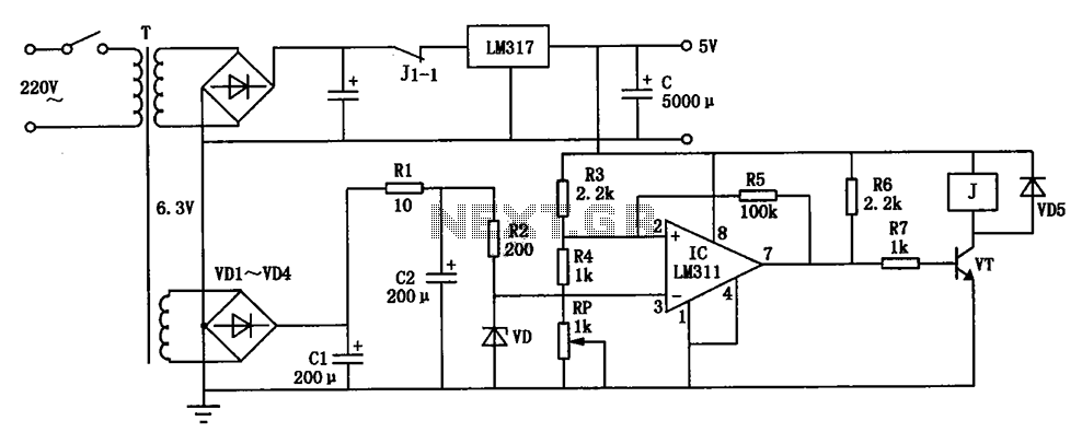
The circuit depicted can be utilized to operate at a voltage of +5V for Single Board Computer (SBC) power, preventing damage caused by over-voltage from the power supply throughout the SBC. This circuit serves as a protective mechanism for Single...

This current-limiting circuit, illustrated as part of a small bench power supply, can be utilized with any dual-rail current source. The section of the circuit on the left limits the current entering the dual voltage regulator (IC4 to IC7)...
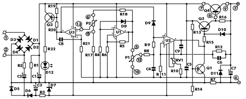
This is an aerial current power supply with a continuously adjustable stabilized output ranging from 0 to 30VDC. The circuit also incorporates an electronic current limiter that effectively controls the output current from a few milliamperes (2 mA) to...
The circuit depicted is utilized in a power supply system to promptly disconnect the power supply in the event of an over-voltage condition during either the grid's on or off phase, thereby protecting the power capacitors. This circuit serves a...
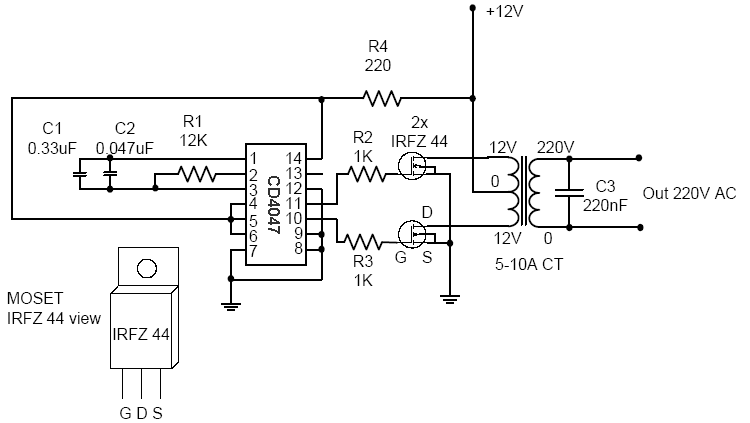
This circuit is very simple, consisting of fewer than 12 components, designed to build a DC to AC converter. The principle of this circuit involves generating a 50/60Hz frequency using the IC CD4047. The output from pins 10 and...
An even power device is designed to supply energy to a computer. It is typically intended for converting alternating current (AC) into low-voltage direct current (DC). Without this component, a computer is merely a collection of metal and plastic...
Warning: include(partials/cookie-banner.php): Failed to open stream: Permission denied in /var/www/html/nextgr/view-circuit.php on line 713
Warning: include(): Failed opening 'partials/cookie-banner.php' for inclusion (include_path='.:/usr/share/php') in /var/www/html/nextgr/view-circuit.php on line 713