
simple precision current source circuit
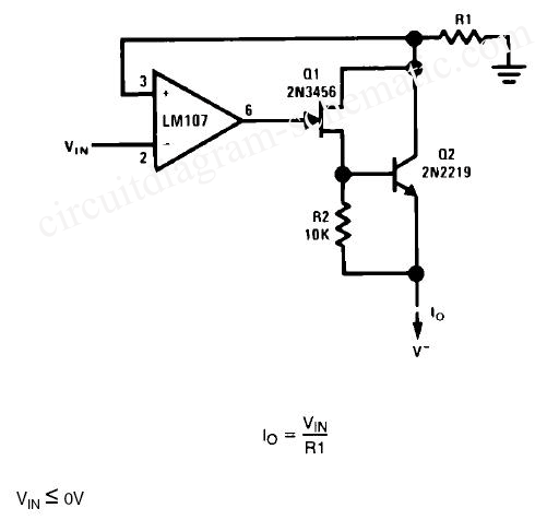
Current generators are critical components in various electronic applications, providing a stable output current that is largely independent of load variations. In this design, the use of a Field Effect Transistor (FET) to drive a bipolar output transistor allows for a high input impedance, which is advantageous for minimizing the loading effect on the preceding circuit stage. The FET operates in the saturation region, ensuring that it can handle small input signals without distortion, thus preserving the integrity of the output current.
In scenarios where output current demands are elevated, a Darlington pair can be utilized as an alternative to the FET-bipolar configuration. This arrangement consists of two bipolar junction transistors (BJTs) connected together, which significantly amplifies the input current. The Darlington configuration is particularly useful for applications requiring high current gain, as it allows for a small input current to control a much larger output current without introducing considerable error due to base current draw.
Compensation of the amplifiers is essential to ensure stability and prevent oscillations at unity gain. This involves adjusting the feedback network to account for phase shifts introduced by load reactance and the characteristics of the external transistors. The compensation technique may vary depending on the specific application requirements, including the frequency response and dynamic behavior of the circuit.
The schematic diagram associated with this design would typically illustrate the interconnections between the FET, bipolar transistor, and compensation networks, providing a visual representation of the circuit's operation. Key parameters such as input and output voltages, bias currents, and load conditions would also be indicated to facilitate a comprehensive understanding of the system's performance.The impedance of these current generators is essentially infinite for small currents and they are accurate so long as VIN is much greater than VOS and IO is much greater than I bias. The source use an FET to drive a bipolar output transistor. It is possible to use a Darlington connection in place of the FET-bipolar combination in cases where the o
utput current is high and the base current of the Darlington input would not cause a significant error. The amplifiers used must be compensated for unity-gain and additional compensation may be required depending on load reactance and external transistor parameters.
Here is a schematic drawing : 🔗 External reference
Related Circuits
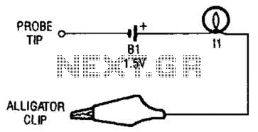
The continuity tester consists of a battery and a lamp connected in series, with one end of the circuit terminated with an alligator clip and the other end connected to the probe tip. The continuity tester is a fundamental...
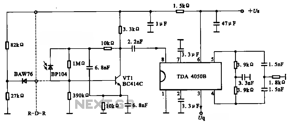
The circuit depicted is an infrared receiver circuit. It primarily consists of an infrared remote control signal switching circuit, designated as VRI, along with signal amplification, filtering, and rectifying integrated circuits, specifically the TDA4050B. The BP104 component serves as...
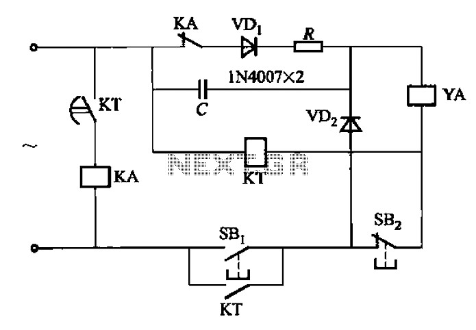
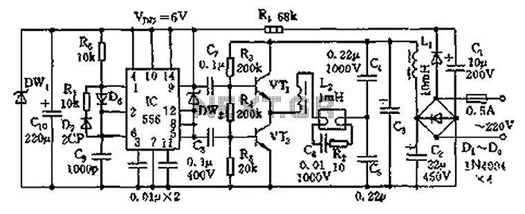
AC solenoid DC circuit operation operates similarly to a DC contactor circuit, but the AC solenoid pull circuit is illustrated in the provided figure. The capacitance C is generally between 1-10 microfarads (µF), with a minimum of 20 microfarads...
The circuit operates as an electronic ballast for fluorescent lamps, incorporating a rectifier filter circuit, a high-frequency oscillation circuit, and an output circuit. The rectifier filter circuit consists of a rectifier diode (VD1) and filter capacitors (C1, C2). The...
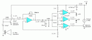
This decibel meter circuit responds to sound pressure levels ranging from approximately 60 to 70 dB (decibels). The sound is captured by an 8-ohm speaker and amplified using a transistor stage along with an LM324 operational amplifier section. A...
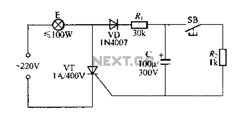
Figure 57 illustrates a simple delay lamp circuit that connects to lamp E using a two-wire connection. This design allows for the security bars to be installed directly, enabling replacement with a standard wall switch without altering the existing...