
Simple Pyro RF Transmitter (27 MHz) Circuit
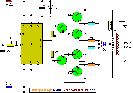
The circuit schematic represents a compact design that efficiently integrates multiple functionalities within a limited space. The mixing of signals at the base of transistor T2 is a critical operation, as it allows for the modulation of the RF transmission signal. The careful selection of through-hole components is essential to maintain the integrity of the circuit while maximizing space utilization.
The ground plane is a vital component of the design, as it not only provides a common reference point for all components but also enhances the performance of the antenna. The thickness of the traces is a consideration in the design process, as it can influence the overall performance of the circuit, especially in RF applications. While smaller traces are typically recommended for higher frequency applications to reduce parasitic capacitance and inductance, the chosen width is adequate for the low-frequency operation of this circuit.
The layout also emphasizes the importance of the toner transfer method in PCB fabrication, where the reversed text is a common occurrence. This method requires careful attention to detail to ensure that the final product meets design specifications. The integration of additional features, such as the PyroElectro.com text, demonstrates the flexibility of the PCB design process and the ability to incorporate branding or identification into the layout without compromising functionality. Overall, the schematic effectively illustrates a well-thought-out design that balances complexity and simplicity in its execution.The schematic for this project is actually deceivingly simple compared to the complexity of what is happening in the circuit. So take a look below or click to view the full sized schematic. The two signals we`ve just generated are mixed together at the base of T2 and once it goes out of the collector of the transistor our continuous wave RF trans
mission signal is ready. The board layout was done in a way so that everything was crammed together very tight. This is a difficult thing to do with through-hole parts, but not impossible. A ground plan covers the entire board (but is chopped up by the traces) so that all parts that need access to ground can have it easily. The ground plan is also very important as its acts as part of our antenna. I just chose a nice thick width that would transfer over nicely when building the PCB, however smaller trace widths seem to be a better choice when designing RF circuits.
but at these low frequencies I don`t believe there will be any performance benefit. My PC board had extra space so I plugged in PyroElectro. com. You`ll notice the text is backwards, this is because during the toner transfer process, a bottom layer is technically printed out backwards, but once on the PCB it reads correctly. 🔗 External reference
Related Circuits
An infrared (IR) sensor or detector circuit diagram utilizing a 555 integrated circuit (IC), primarily employed as a water level or liquid level sensor and proximity detector circuit. The described circuit employs a 555 timer IC configured in a monostable...
The relay control allows for multiple pairs of contacts to be connected in parallel, enabling the circuit to handle a large lamp power. The design is straightforward; by simply changing the capacitance of the capacitor, different flash frequencies can...

The monostable flip flop, sometimes called a 'one shot' is used to produce a single pulse each time it is triggered. It can be used to debounce a mechanical switch so that only one rising and one falling edge...
This circuit illustrates a precision digital timing control system. The controller includes a crystal oscillator circuit, a divider, a counting circuit, and monostable flip-flops. The crystal oscillator circuit features a series of 14 binary counters/dividers, a watch crystal operating...
This document describes a 100 Watt inverter circuit that utilizes a minimal number of components. The circuit employs the CD 4047 integrated circuit (IC) from Texas Instruments to generate 100 Hz pulses, along with four 2N3055 transistors that drive...
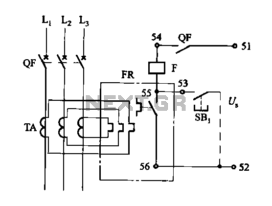
The DK-5A, 5D, and SDb control boxes are equipped with a thermal electromagnetic overcurrent release, as depicted in Figure 6-80. The trip mechanism provides both overload and instantaneous short circuit protection with a long delay feature. In the figure,...
Warning: include(partials/cookie-banner.php): Failed to open stream: Permission denied in /var/www/html/nextgr/view-circuit.php on line 713
Warning: include(): Failed opening 'partials/cookie-banner.php' for inclusion (include_path='.:/usr/share/php') in /var/www/html/nextgr/view-circuit.php on line 713