
simple supply voltage monitor
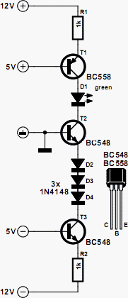
The described voltage monitoring circuit employs a straightforward design that leverages the characteristics of bipolar junction transistors (BJTs) to provide a reliable indication of supply voltage integrity. The circuit operates within a dual voltage range, monitoring both positive and negative supply lines, specifically ±5 V and ±12 V. The configuration includes two primary transistors, T1 and T3, which are configured as current sources, ensuring stable operation across varying load conditions.
Resistors R1 and R2 play a crucial role in setting the reference voltage drop across the circuit, calculated to be 6.3 V. This voltage drop is essential for maintaining the necessary biasing conditions for the transistors. The current flowing through these resistors is measured at 6.3 mA, which is adequate to activate diode D1 under normal operating conditions, indicating that all monitored voltages are present.
In the event of a failure in the 5 V supply line, the circuit is designed to respond effectively. Transistor T3 continues to conduct, maintaining its state; however, the failure impacts transistor T2's base-emitter junction, which loses its bias. As a result, T2 ceases to conduct, interrupting the current flow through diode D. This change serves as an indication of the fault condition, effectively signaling that one of the critical supply voltages is no longer available.
Overall, this voltage monitoring circuit provides a robust and efficient solution for ensuring the integrity of ±5 V and ±12 V supply lines, utilizing minimal components while maintaining clear operational functionality. The design's simplicity enhances reliability and reduces potential points of failure, making it suitable for various applications in electronic systems where voltage monitoring is essential.A circuit for monitoring supply voltages of ±5 V and ±12 V is readily constructed as shown in the diagram. It is appreciably simpler than the usual monitors that use comparators, and AND gates. The circuit is not intended to indicate the level of the inputs. In normal operation, transistors T1 and T3 must be seen as current sources. The drop acr oss resistors R1 and R2 is 6. 3 V (12 5 0. 7). This means that the current is 6. 3mA and this flows through diode D1 when all four voltages are present. However, if for instance, the 5 V line fails, transistor T3 remains on but the base-emitter junction of T2 is no longer biased, so that this transistor is cut off. When this happens, there is no current through D which then goes out. 🔗 External reference
Related Circuits
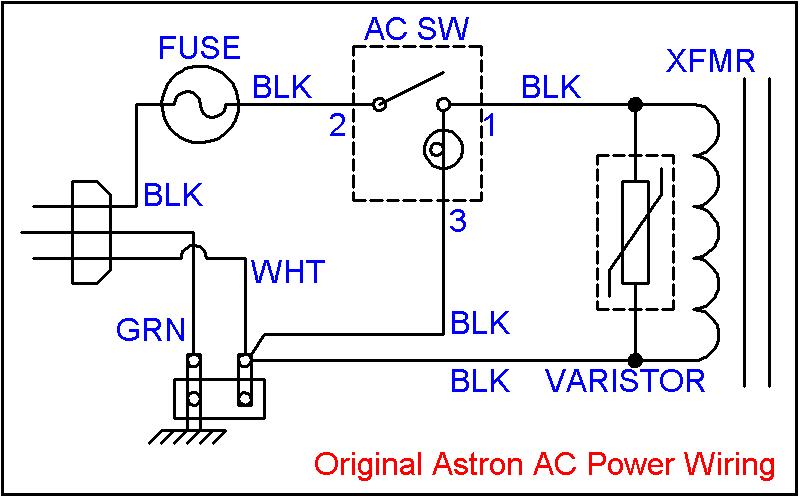
Owners of large 500-watt and higher Astron linear power supplies, as well as large HF amplifiers, are familiar with the "GNNNNnng" sound that occurs upon power-up. This noise is caused by the high inrush (surge) current flowing into the...
This document outlines a simple PWM (Pulse Width Modulation) DC to AC voltage inverter circuit based on the SG3524 integrated circuit. The SG3524 is a fixed frequency PWM voltage regulator control circuit that offers indifferent outputs suitable for both...
The NE568A (NE568AD, NE568AN, SA568AD, SA568AN) is a monolithic phase-locked loop (PLL) that operates from 1Hz to frequencies exceeding 150MHz. It features an extended supply voltage range and a lower temperature coefficient of the VCO center frequency compared to...
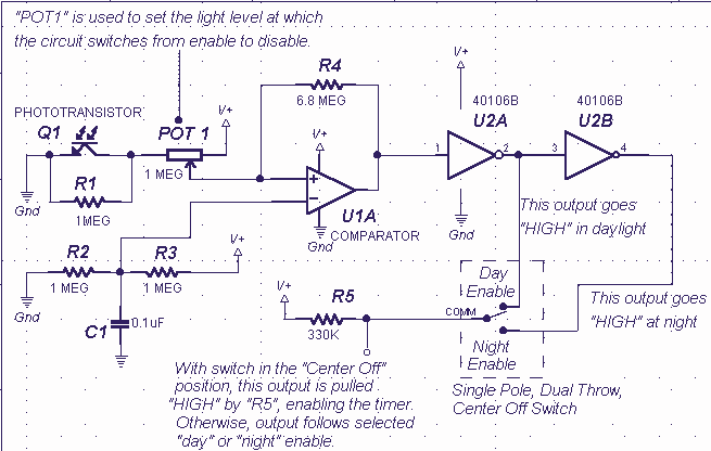
This is a simple circuit that does the day/night switchings you have in mind. POT1 is used to set the light level at which the circuit switches from enable to disable. The described circuit functions as an automatic day/night switch,...
This chapter provides detailed schematics of various power supplies suitable for use with common Ar/Kr ion tubes available to hobbyists in the surplus market. Included are examples of commercial designs (Omnichrome 150R and 532 head, Lexel 88 and head)...

The under/over voltage protection circuit with time delay presented here is a low-cost and reliable circuit for protecting equipment from damage. This under/over voltage protection circuit is designed to safeguard electronic equipment from voltage fluctuations that can lead to potential...