
Single Chip Stereo FM Transmitter Circuit

An FM transmitter circuit typically consists of two main components: the FM modulator and the RF amplifier. The FM modulator is responsible for varying the frequency of a carrier wave in accordance with the input audio signal, which is often a composite signal that combines multiple audio channels. This modulation process enables the transmission of audio information over radio frequencies.
The RF amplifier serves to boost the power of the modulated signal to ensure it can be effectively transmitted through an antenna. The output power of the RF amplifier is crucial, as it determines the transmission range of the FM signal. The schematic diagram of the FM transmitter circuit illustrates the interconnection of these components, including the input for the audio signal, the modulator circuit, and the RF amplifier stage.
In a typical design, the FM modulator may utilize a varactor diode or a phase-locked loop (PLL) to achieve frequency modulation. The modulator's output is then fed into the RF amplifier, which may be a class C amplifier for efficient power handling. The antenna is connected to the output of the RF amplifier, allowing the modulated signal to be radiated into the environment.
Additional components such as filters may be included in the circuit to eliminate unwanted harmonics and ensure signal clarity. Proper design considerations should be made regarding the power supply, component ratings, and PCB layout to minimize interference and maximize performance. Overall, the FM transmitter circuit is a sophisticated assembly of electronic components designed to facilitate the wireless transmission of audio signals.an FM modulator that modulate a carrier frequency with the composite signal, and an RF amplifier that provide enough power to be transmitted through antenna. Here is the schematic diagram of theFM transmitter circuit: The core of this stereo FM tra.. 🔗 External reference
Related Circuits
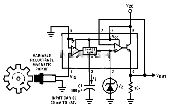
After each zero electromagnetic pickup receives a sine wave input, as illustrated in the National Semiconductor LM2907 circuit, it generates an output pulse. This circuit can be utilized in digital control systems. The width of each pulse corresponds to...
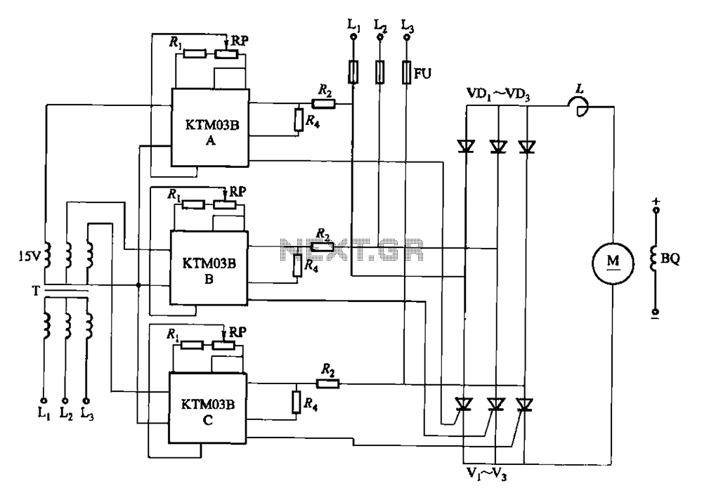
Adjusting the phase potentiometer RP can change the conduction angle of each corresponding thyristor (V1-V). This adjustment alters the voltage applied across the load. The circuit utilizes a phase control technique to manage the power delivered to a load by...

This is a simple circuit design for a video transmitter capable of radiating signals up to 50 meters. The video transmitter can be connected to a camera as a source and allows viewing on a VHF channel analog television....
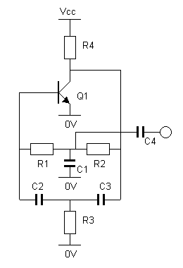
The output of this circuit should be connected to a high-impedance load, typically greater than 100K ohms, while noting that the impedance of capacitor C4 is approximately 3K ohms. A PNP transistor may also be utilized, requiring adjustments to...
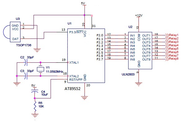
The infrared (IR) circuit is designed to control multiple devices using a TV remote. Unlike standard circuits that can typically switch only one device, this circuit allows for the operation of different devices with the same remote by utilizing...
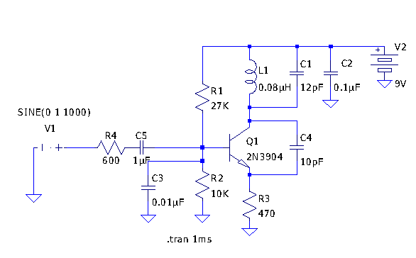
Tetsuo Kogawa's circuit is well documented, although not in a conventional schematic form. It has been entered into LTSpice for analysis, and the schematic is presented online with some comments. The circuit includes a small air variable capacitor (C1)...