
siren alarm circuit diagram usng lm358
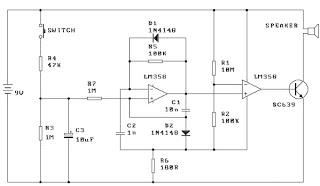
The circuit operates effectively as a timing and pulse generation mechanism, utilizing the charging and discharging characteristics of capacitors C3 and C1, along with the feedback and control features of the op-amp 358. The time constants associated with the resistors and capacitors play a critical role in determining the timing behavior of the circuit. The op-amp's configuration allows it to function as a pulse generator, where the interplay between the control voltage on C3 and the discharge characteristics of C1 dictate the timing of the output pulse.
As the switch is engaged, the rapid charging of C3 through R4 initiates the timing cycle. The slow discharge through R7 and R3 creates a delay, allowing for a controlled increase in voltage at pin 5. Once the threshold is reached, the op-amp's output transitions, generating a pulse that is utilized for further circuit functions. The recharging of C3 through D2 is a crucial aspect of the circuit, as it ensures that the op-amp can reset itself quickly after each pulse generation, maintaining the oscillatory behavior.
The use of R5 and C2 is particularly important for shaping the output pulse. By delaying the rise time at pin 6, the circuit can ensure that the output pulse is well-defined and has the necessary duration for downstream applications. This design allows for flexibility in adjusting the timing characteristics by varying the resistor and capacitor values, making it suitable for a range of applications requiring precise timing and control.When the switch is pressed C3 charges up through R4 with a time constant of 0. 47 seconds and when the switch is released C3 begins a slower discharge through R7 and R3 with a time constant of about 5 seconds. The op amp 358 used in this project is set up as a voltage controlled oscillator. When the output of the oscillator (pin 7) switches low the re is a charge remaining in C1 which holds pin 5 below the switching point. Current through R7 is proportional to the control voltage on C3. This current discharges C1 causing the voltage on pin 5 to rise towards the switching point at a rate proportional to the voltage on C3. When the switching point is reached pin 7 switches high and initially pulls pin 6 high via C1. This causes the op amp to temporarily turn on hard. But C3 quickly recharges through D2 causing the voltage on pin 5 to fall below the switching point and causing the op amp to switch off again.
The positive pulse output from the op amp puts a fixed amount of charge into C2 slightly raising the potential of pin 6. This causes the potential on pin 6 to rise and assist the sharp switch off of the op amp. Also R5 & C2 delay the rise on pin 6 long enough to get a good output pulse. 🔗 External reference
Related Circuits
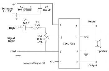
This is an audio amplifier circuit that uses the TDA7052 as the main component, along with five additional components to support its operation. The ideal supply voltage for this circuit is approximately 6-12V, and it does not require a...
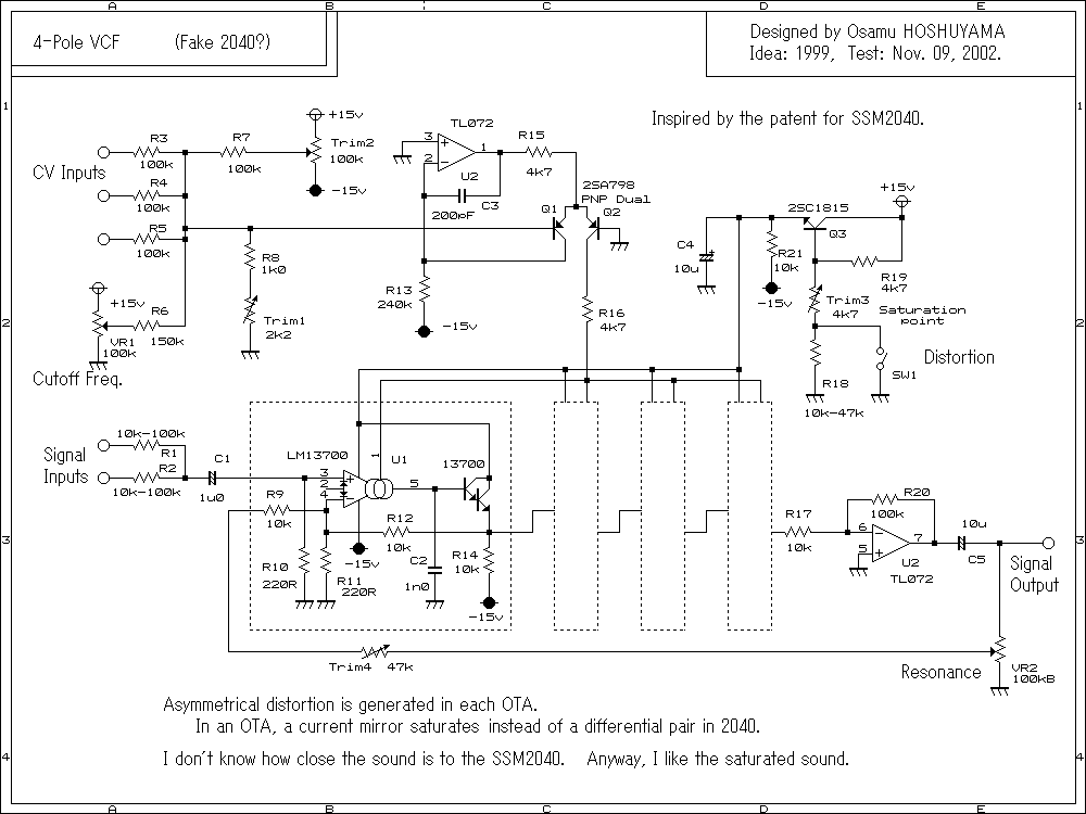
The initial intention was to name the product "Chimera," but due to an existing synth company with that name, it was decided to use "Cerberus" to avoid confusion. The term "Tricephalic Filter" was deemed less appealing. Similar to its...
A pulse booster circuit is utilized to increase the pulse amplitude. The structure illustrated in figure (a) of the circuit can output a pulse amplitude that is twice that of the input. Figure (b) of the circuit can achieve...
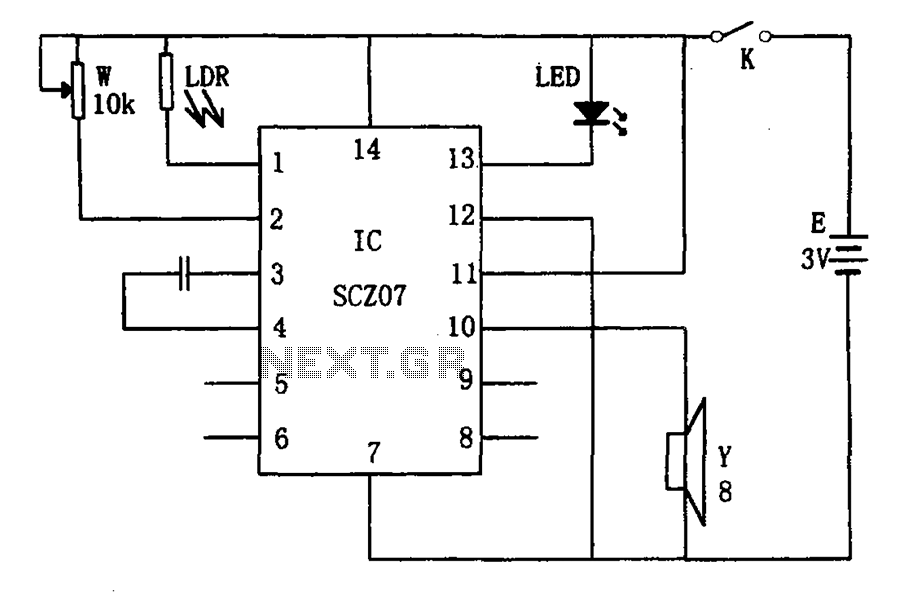
The weak light alarm circuit is illustrated in the figure. The oscillator circuit's core component is the SCZ07. The input signal is controlled by a potentiometer (W) and the output signal is processed by a photoresistor (LDR). The circuit...
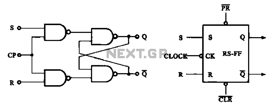
The asynchronous RS flip-flop mentioned earlier is not synchronized with the system clock signal. In contrast, the synchronous RS flip-flop incorporates synchronization, allowing it to operate in conjunction with the clock signal. Figure (a) illustrates the circuit configuration of...
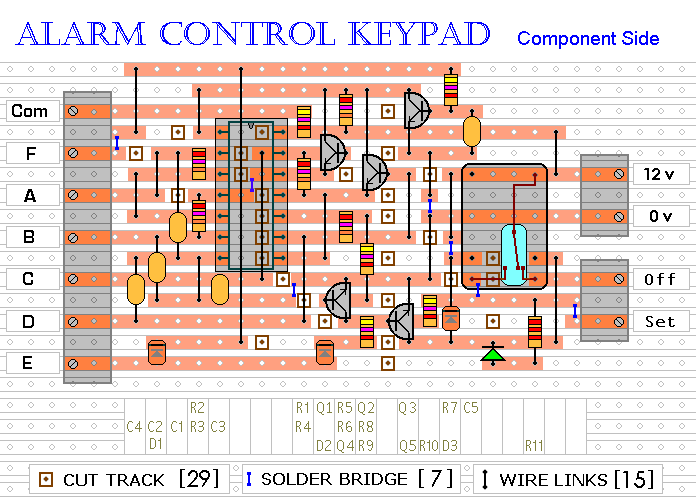
This keypad is designed for use with a modular burglar alarm system but can also be applied in various other applications. Pressing a single key will activate the relay, while entering a four-digit code of your choice will deactivate...
Warning: include(partials/cookie-banner.php): Failed to open stream: Permission denied in /var/www/html/nextgr/view-circuit.php on line 713
Warning: include(): Failed opening 'partials/cookie-banner.php' for inclusion (include_path='.:/usr/share/php') in /var/www/html/nextgr/view-circuit.php on line 713