
Smart Turn Signal Circuit

The STS circuit serves as an essential reminder for drivers to turn off their turn signals, thereby enhancing road safety. The operation begins with the charging of capacitor C3, which is influenced by the signal from the turn signal flasher circuit. The gradual increase in voltage at the gate of Q2 allows it to switch on, initiating the buzzer activation sequence after the predetermined time interval.
The circuit's design incorporates key components such as the integrated circuit IC1, which is responsible for generating the timing signal, and the C1-R2 combination that sets the time constant for the output signal duration. The design ensures that the buzzer's loudness can be controlled through a current-limiting resistor, allowing for a customizable warning sound that is audible but not overly disruptive.
The connection points within the circuit, including point A for the flasher signal, point C for the IC output, and point D for the voltage monitoring, are strategically placed to facilitate easy troubleshooting and integration into existing vehicle electrical systems. The use of a brake-on signal to disable the buzzer when the vehicle is stationary is a thoughtful inclusion that prevents unnecessary distractions for the driver.
Overall, the STS circuit exemplifies a practical application of electronic components to improve driver awareness and vehicle safety, making it an invaluable addition to modern automotive designs. STS schematic. The Q2 gate voltage increases with the charge on C3. After 15 seconds of charging, the buzzer will warble. As the charging continues, the sound will grow louder.Circuit waveforms. Point A shows the signal from the flasher. The voltage at point D will increase as long as the pin-3 output of IC1 (point C) remains high. The C1-R2 time constant (point B) determines how long the output will be high.Flasher terminal L connects to the load and X connects to the 12-volt supply. When the driver engages the turn signal, the L terminal voltage varies with the blinking lights. The STS senses the changing voltage and, after 15 seconds, it applies power to a buzzer through a current-limiting device to control loudness.
This circuit reminds a driver that his turn signal has been left on for more than 15 seconds. When stopped for a light, the brake-on signal holds the warning off.
Related Circuits
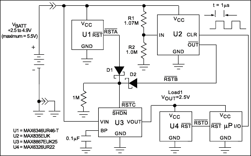
The micropower circuit automatically provides shutdown, power-up, and low-battery lockout functions without requiring software or operator control. The micropower circuit is designed to manage power efficiently in battery-operated devices, ensuring optimal functionality while conserving energy. The shutdown feature is activated...

The circuit utilizes an IRF740 MOSFET, which has a maximum drain-source voltage (V_DS) rating of 400V. The avalanche voltage is calculated to be approximately 3520V, indicating that up to about 500V of inductive kickback voltage can develop in the...

This circuit illustrates an automatic unattended burglar alarm system designed primarily for residential use, warehouses, and similar applications. The circuit features a pyroelectric infrared sensor integrated with a light control mechanism. It comprises components such as resistors (RG, RP2,...

The circuit consists of two synchronized multivibrators formed by a pair of 555 timer circuits. It is capable of generating two synchronized pulse signals, with the spacing and frequency adjustable by modifying the time constant. The circuit offers flexibility...

The Meter Ml is a +/-50-uA zero-center D'Arsonval meter movement driven by Ul, a TL081 FET op amp, through R3. The gain of Ul is set to 11 using resistors R1 and R2, while capacitor C1 restricts the bandwidth...
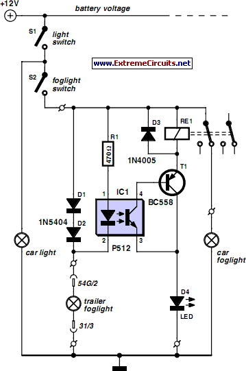
A rear fog lamp is mandatory for trailers and caravans to enhance visibility during foggy conditions. When the fog lamp is activated, the fog lamp of the towing vehicle must be turned off to prevent distracting reflections. To achieve...