
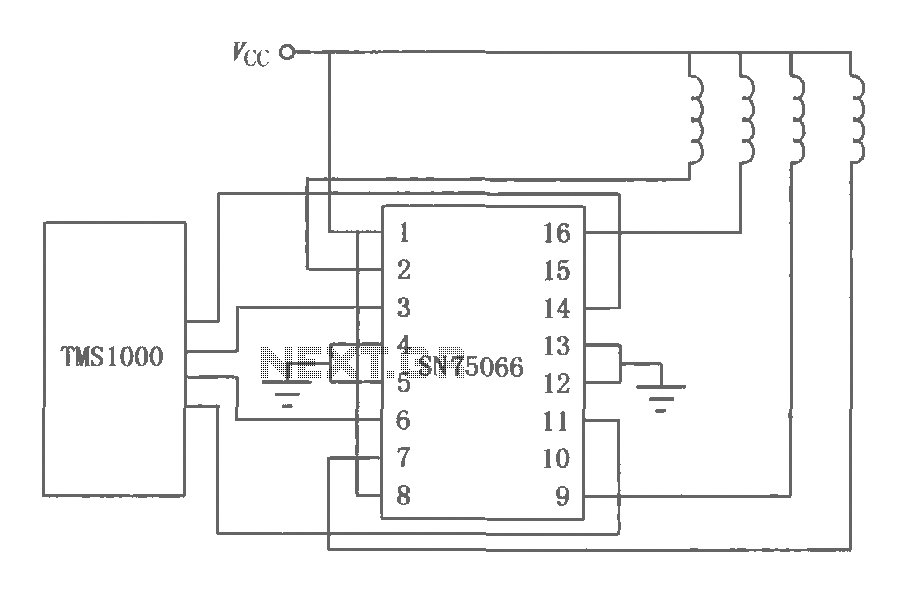
SN75064 ~ SN75067 current Darlington circuit diagram of a switch
The SN75064 to SN75067 series is engineered to handle demanding electrical loads, making it ideal for applications requiring robust switching capabilities. The Darlington configuration enhances current gain, allowing these devices to efficiently drive higher currents while maintaining low input current requirements. The integration of clamp diodes serves to protect the circuit from voltage spikes that can occur when switching inductive loads, thus improving the reliability of the system.
The capability of paralleling multiple Darlington pairs within a single package allows for increased current handling, which is particularly beneficial in applications such as motor control, solenoid actuation, and other inductive load scenarios. The output current specification of 1.5A ensures that these devices can effectively manage substantial loads without overheating, while the 2W power rating provides a margin for safe operation under various conditions.
Compatibility with both TTL/DTL and CMOS logic levels enables flexibility in design, allowing engineers to integrate these switches into existing systems without significant redesign. The SN75064 and SN75065 are optimized for low-voltage digital applications, while the SN75066 and SN75067 cater to high-voltage requirements, expanding the range of potential applications.
In designing circuits that utilize the SN75066, it is critical to consider the delay drive interface, which can be implemented using a standard configuration to ensure proper timing and functionality. This design consideration is essential for applications that require precise control over switching times, such as in timing circuits or sequential logic applications.
Overall, the SN75064 to SN75067 series provides a versatile solution for high-voltage and high-current switching needs, combining durability, efficiency, and adaptability for a wide range of electronic applications.SN75064 ~ SN75067 is a monolithic, high-voltage, high-current Darlington switch output termination has clamp diodes, suitable inductive loads. Each package of four Darlington pair can be used in parallel, so you can obtain further large current output. The chip output current up to 1.5A, rated power 2W, high voltage output, with output clamping diodes to the common emitter current absorption circuit.
Wherein the input SN75064 / 75065 is compatible with TTL, DTL and 5V CMOS circuit; input SN75066 / 75067 is compatible with PMOS and high voltage CMOS circuit. By SN75066 for delay drive interface should use typical circuit is shown.
Related Circuits
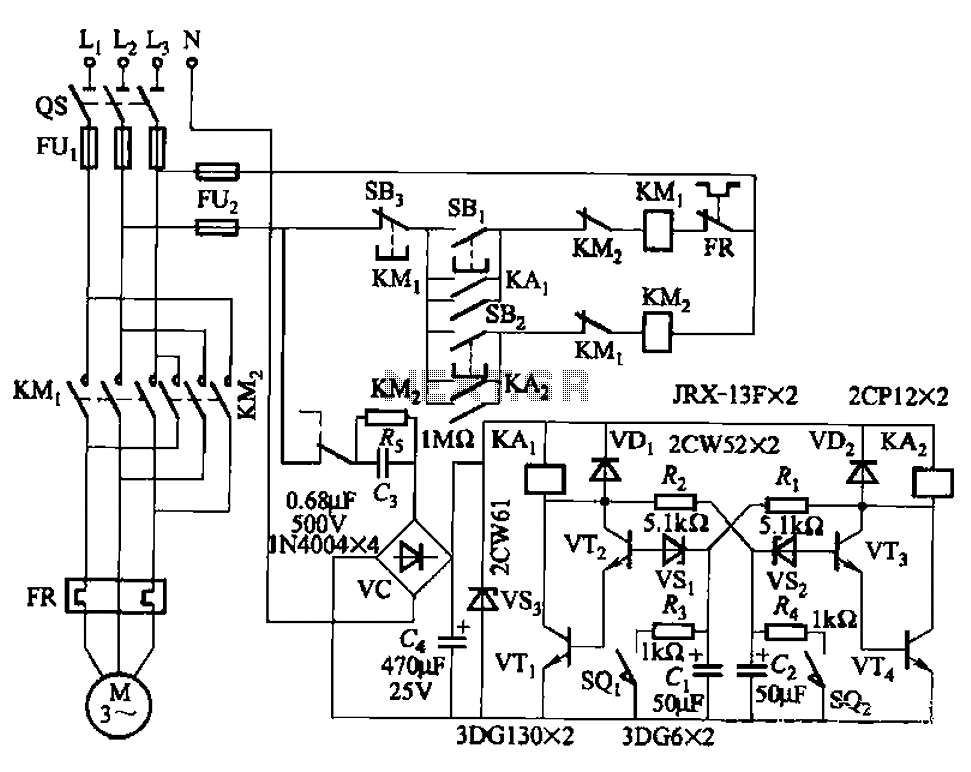
The circuit illustrated in Figure 3-72 employs a deformable bistable reversing motor control mechanism that automatically initiates and halts operation during a user-defined time delay. This feature is designed to safeguard the motor from potential impacts during the reversing...
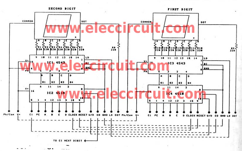
This is a versatile digital counter circuit that is cost-effective due to the basic components available in many electronic shops. The digital counter circuit is designed to count pulses and display the count on a digital readout, typically using a...
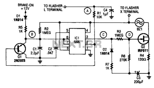
The STS schematic illustrates a circuit designed to alert a driver when the turn signal has been active for more than 15 seconds. The voltage at the gate of transistor Q2 increases in response to the charge accumulated on...

Alarm system designs often require circuitry that can detect whether a phone line is active or broken. The primary challenge in this design is to draw less than 5 µA from the phone line, which operates within a voltage...

This Project REMOTE CONTROLLED SWITCH BOARD is used to switch on/off the Home Appliances by using a standard Remote control. The system is used to switch on/off up to six electrical devices. All the above processes are controlled by...

This circuit for an intercom is a stand-alone electronic communications system designed for limited or private dialogue. The schematic illustrates the application circuit of the LM390 in the intercom configuration. Gain control can be achieved by capacitively coupling a...