
solar battery charger circuit schematic
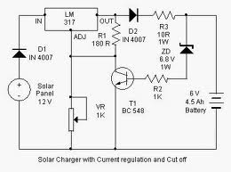
The described circuit operates as a battery charger with adjustable output voltage and current regulation. The Adjust pin serves as a control point for the charging voltage, and the variable resistor (VR) allows fine-tuning of this voltage to ensure optimal charging conditions for the battery, which is set at 9 volts in this configuration.
The inclusion of resistor R3 is critical as it restricts the charging current to a safe level, preventing potential damage to the battery from excessive current. The diode D2 plays an essential role in maintaining the integrity of the charging circuit by blocking reverse current flow, thus ensuring that the battery does not discharge back into the charger when it is not in operation.
Transistor T1 is utilized as a switch in conjunction with the Zener diode ZD. Under normal operating conditions, T1 remains in the off state, allowing the charging current to flow to the battery. However, when the battery's terminal voltage rises above the Zener voltage of 6.8 volts, ZD begins to conduct, providing sufficient base current to turn on T1. This action effectively disconnects the charging current from the battery, preventing overcharging and ensuring the longevity of the battery.
Overall, this circuit design emphasizes safety and efficiency in battery charging, leveraging components such as resistors, diodes, and transistors to create a reliable and adjustable charging solution. Proper selection of components and values is crucial to achieving the desired performance and protecting both the battery and the charging circuit.By adjusting its Adjust pin, output voltage and current can beregulated. VR is placed between the adjust pin and ground to provide an output voltage of 9 volts tothe battery. Resistor R3 Restrict the charging current and diode D2 prevents discharge ofcurrent from the battery.
Transistor T1 and Zener diode ZD act as a cut off switch whenthe battery is full. Normally T1 is off and battery gets charging current. When the terminal voltage of the battery rises above 6. 8 volts, Zener conducts andprovides base current to T1. 🔗 External reference
Related Circuits

The following circuit illustrates the AD8531 integrated circuit used for the automatic control of LCD panel backlighting. Features include the ability to compensate for aging effects and other functionalities. The AD8531 is a precision operational amplifier known for its low...
Chaolitong Phone Travel Charger for Motorola models 308, 328, 338, and 368 series mobile phone batteries. This charger features a switch for nickel-cadmium, nickel-hydrogen, and lithium-ion batteries, along with a discharge function. It operates with an AC mains input...
Circuit audio peak indicator circuit schematics. Circuit Electronics, schematics for audio peak indicator circuit. An audio peak indicator circuit is designed to visually represent the peak levels of an audio signal, providing critical information for audio engineers and musicians regarding...
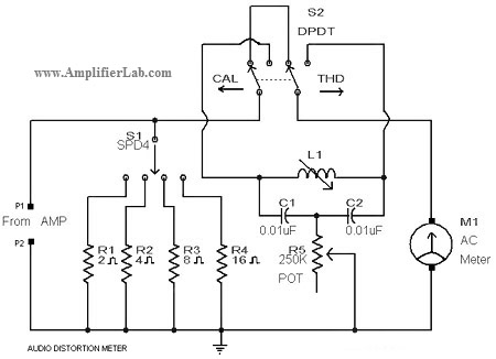
A circuit diagram of an audio distortion meter is presented here. An audio distortion meter is utilized to measure Total Harmonic Distortion (THD). The audio distortion meter is an essential tool in audio engineering, designed to quantify the level of...
The two unspecified polarized capacitors (one directly above the transformer and one directly to the right of the transformer) are actually each a pair of 470 µF capacitors in parallel (for a total of four 470 µF capacitors). These...
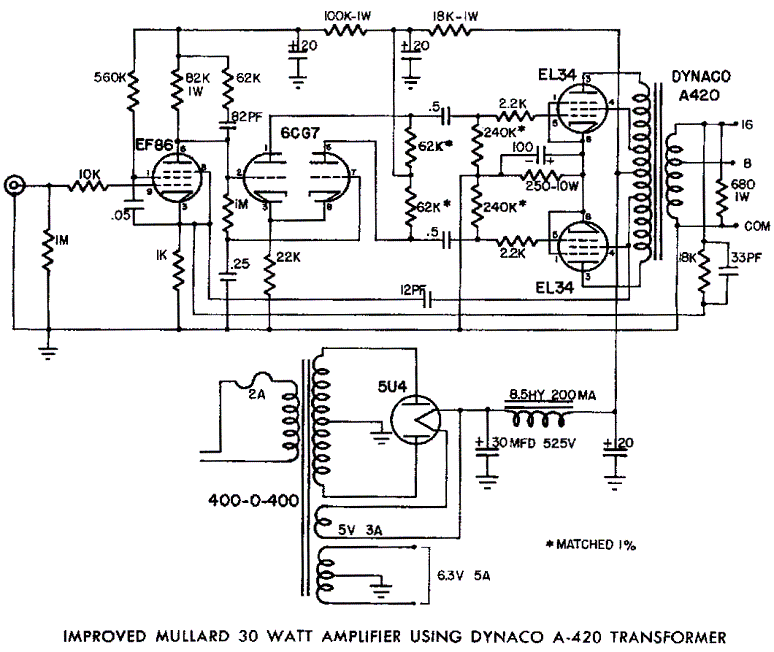
Mullard EL34 push-pull vacuum tube amplifier schematic using Dynaco A420 audio output transformers The Mullard EL34 push-pull vacuum tube amplifier is a classic audio amplification circuit that utilizes EL34 vacuum tubes in a push-pull configuration to deliver high-quality sound reproduction....