
Sound field effect transistor amplifier circuit
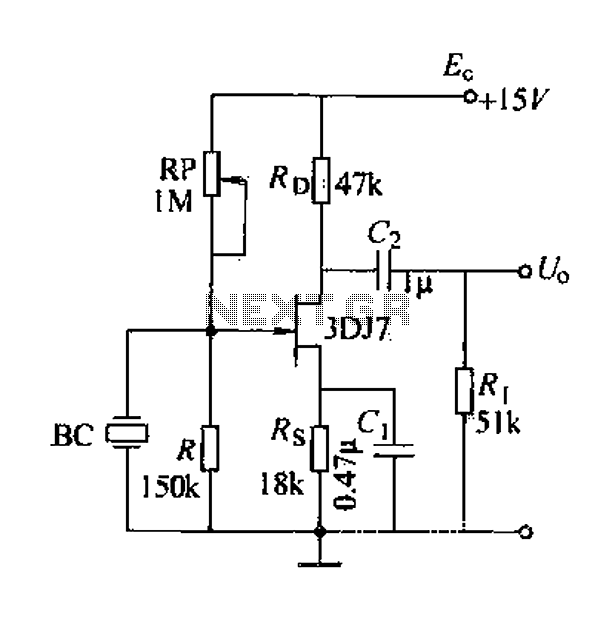
A field effect transistor (FET) voice amplifier is an essential component in audio applications due to its high input impedance and low noise characteristics. The low input impedance of approximately 1 kΩ necessitates a constant current signal from the source, which is crucial for the stable operation of the amplifier. FETs, as voltage-controlled devices, operate by varying the voltage at the gate terminal, which influences the conductivity between the source and drain terminals without drawing significant current from the input signal.
The high input impedance (10^7 Ω) of FETs minimizes the loading effect on preceding stages in a circuit, allowing for better signal integrity and fidelity. This characteristic, combined with low noise and high gain, makes FETs particularly advantageous in applications requiring precise amplification, such as in audio processing and signal conditioning circuits.
In typical configurations, such as the common source amplifier illustrated, the gate (G) is coupled to the source (S), while the drain (D) is reverse-biased. This configuration enables the FET to amplify input signals effectively. The drain resistance (Rn) plays a critical role in determining the voltage gain of the amplifier; a higher drain resistance allows for greater voltage swings, resulting in improved amplification.
The biasing of the gate is achieved through a resistor network, which establishes the appropriate gate voltage for optimal performance. The use of an adjustable resistor (RP) in the gate biasing circuit allows for fine-tuning of the quiescent point, ensuring the amplifier operates within its linear region. This adjustability is vital for accommodating variations in component tolerances and maintaining consistent performance across different operating conditions.
In summary, the FET voice amplifier is a versatile and effective solution for audio amplification, leveraging its high input impedance, low noise, and adjustable biasing to deliver reliable performance in a wide range of electronic applications.Field effect transistors voice amplifier, the input impedance of the transistor is low, only lkCZ, requiring signal source provides a constant current signal to work. The field effect transistor is not, it is a voltage-controlled device, within the normal working range of Si, the gate G a few take almost no current. Field effect transistor has a very high input impedance (107n), low noise, large dynamic range and high magnification, use it usually only composed of a voltage amplifier with level to meet the requirements.
It is widely used in various electronic sub-circuits. Sub-junction field effect transistor and an insulated gate type two, this section describes the junction field effect transistor transistor. Figure is a gate voltage divider type common source amplifier, similar to those in Figure 9-18 common emitter VT1 transistor amplifier.
It works as follows: transistor amplifier and similar circuits, must always be first gate (G) of a source (S) and the gate (G) - drain (D) two IN junction is reverse biased state (for N-type tube ), such as the drain current gate current k change varies, if the drain resistance Rn great, you can get a lot of voltage changes from f and electrical amplification. Its gate bias resistor bias current is not made to its gate, and the gate bias voltage is obtained. To do this in the circuit, it is common bias resistor adjustable resistor RP, easy to obtain when appropriate quiescent point in the circuit to adjust the gate bias.
Related Circuits
The agriculture and electrical power harrow plow power cord must consist of four rubber cables, with one core wire designated as the ground wire. The traction machine housing must be properly grounded. The two traction power machines are connected...
This Korean SuperCap OEM supports usage in series configurations. Consider whether the implementation will be manual or automatic, such as with a smart battery charger or a power fail backup circuit. It is essential to balance the voltage and...
This document discusses the series used in USB connections for charging batteries. The output voltage ranges from 4.7 volts to 5 volts DC, which is suitable for charging mobile phones and other battery types. The circuit described enhances the...
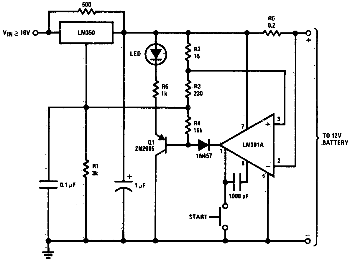
DC 12V Battery Charger Circuit Diagram. This circuit is a high-performance charger for gelled electrolyte lead-acid batteries. The DC 12V battery charger circuit is designed to efficiently charge gelled electrolyte lead-acid batteries, which are commonly used in various applications due...
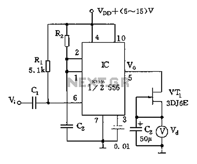
The circuit utilizes switch contacts that are proportional to the speed pulse signal Vi. A differential signal is fed into the trigger side of an integrated circuit (IC), specifically a 555 timer configured in monostable mode (1/2 556), to...
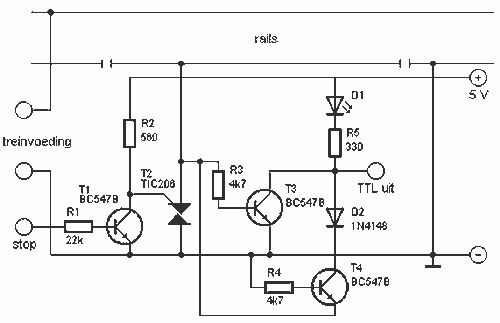
This circuit can detect whether a train is in a particular drive. The output is TTL and CMOS compatible and can be processed by such a computer. The simple circuit works. The driving voltage is connected to the two...