
SPARK GAP OSCILLATOR

The circuit operates by utilizing a high-voltage transformer (T1) that is designed to limit current, ensuring safe operation within the system. The transformer steps up the voltage from a lower-level source to a high-voltage output suitable for charging the capacitor (C1). As C1 accumulates charge, it approaches the maximum voltage output of T1, which is critical for the subsequent operation of the spark gap.
The spark gap serves as a switch that remains open until the voltage across it reaches a certain threshold. Once this threshold is exceeded, the air gap ionizes, allowing current to flow and effectively shorting the LC circuit comprising the inductor (L1) and capacitor (C1). This sudden closure of the circuit leads to a rapid discharge of the stored energy in C1 through L1, generating a significant inductive kick. The inductive kick is characterized by a rapid change in current, which produces a high voltage spike due to the energy stored in the magnetic field of the inductor.
The oscillation of the LC circuit is a result of the interaction between the inductor and capacitor. When energy is transferred from the capacitor to the inductor, it creates an oscillatory behavior defined by the resonant frequency of the LC circuit. This frequency is determined by the values of L1 and C1, which can be adjusted to achieve the desired oscillation characteristics. The circuit is capable of oscillating over a broad frequency range, which can be advantageous in applications requiring wideband performance.
In summary, the described circuit effectively demonstrates the principles of high-voltage transformer operation, energy storage in capacitors, and the dynamic behavior of LC circuits, providing a foundation for various applications in electronics, including RF generation and pulsed power systems.A high-voltage current-limiting transformer (T1) supplies power to the basic LC tuned circuit. As C1 charges to near the transformer`s maximum output voltage, the spark gap`s air space breaks down, completing the circuit between the inductor and capacitor, L1 and C1. The tremendous inductive kick in the circuit is caused by the inductive field col lapse when the spark gap shorts out the LC series circuit. The LC tuned circuit oscillates in a very broadband manner. 🔗 External reference
Related Circuits
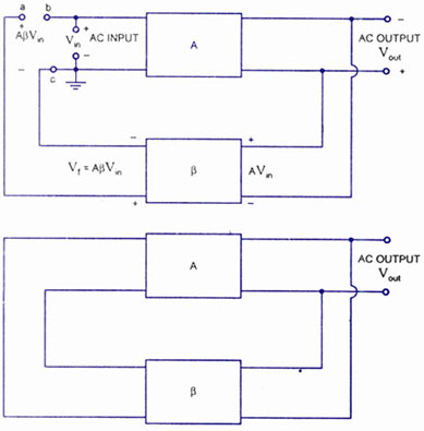
A feedback amplifier with a closed-loop gain, Af, greater than unity can be achieved through the use of positive feedback. This condition also fulfills the phase requirement, leading to the operation of an oscillator circuit. An oscillator circuit generates...
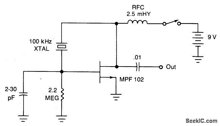
The JFET Pierce oscillator is stable and simple. It can serve as the clock for a microprocessor, a digital timepiece, or a calculator. With a probe at the output, it can be utilized as a precise injection oscillator for...
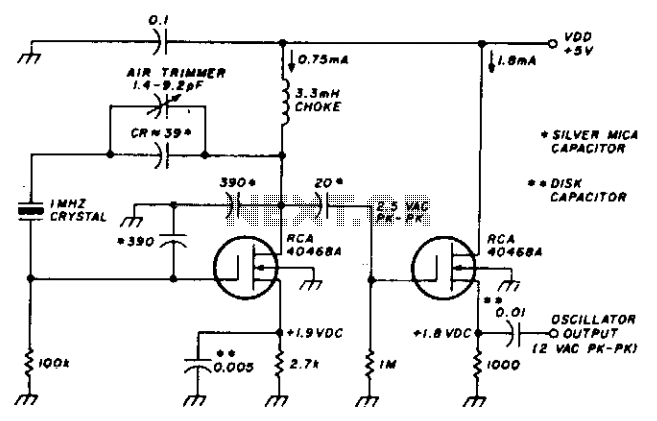
This stable oscillator circuit exhibits less than a 1 Hz frequency change over a VDD range of 3 to 9 volts. Stability is attributed to the use of MOSFET devices and stable capacitors. The described oscillator circuit is designed to...
A 430 MHz transmitter for microwave applications is being constructed, but there is an issue with obtaining any output frequency from the circuit. The construction of a 430 MHz transmitter for microwave applications involves several critical components and considerations to...
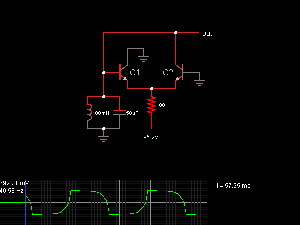
When the oscillator starts, Q2 is in a conducting state; the current flows from the capacitor, charging it until the voltage across it is sufficient to allow current to flow through the inductor. As the current through the inductor...
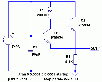
A schematic diagram of the oscillator is presented in Figure 1. The common-base transistor stage (Q1) amplifies the signal within the positive feedback loop. The positive feedback signal develops across the resistor R1, which is shared by the emitters...