
SPDIF audio DAC with CS8416 and TDA1543
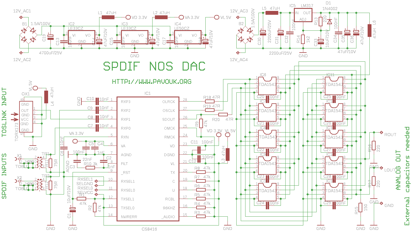
The circuit design emphasizes high-quality audio performance through careful selection of components and isolation techniques. The galvanic separation of electrical inputs ensures minimal noise interference, which is critical for high-fidelity audio applications. The use of pulse transformers for signal isolation not only maintains signal integrity but also provides the necessary impedance matching for the DAC inputs. The choice of the TDA1543 DAC, known for its simplicity and effectiveness, allows for a cost-effective solution that does not compromise sound quality.
The power supply design is crucial, with multiple low-dropout regulators ensuring stable voltage levels for various sections of the circuit. The implementation of tantalum capacitors for voltage filtering enhances the overall performance by providing low equivalent series resistance (ESR), which is beneficial for audio applications. The inclusion of decoupling capacitors close to the chips minimizes voltage fluctuations and noise, further improving the reliability of the circuit.
The hardware and software modes of the CS8416 provide flexibility in operation, allowing for either simple hardware-based solutions or more complex software-driven applications. The internal PLL and external components work together to maintain synchronization across the system, ensuring that audio signals are processed accurately.
The parallel connection of multiple DACs is a strategic choice to enhance audio output precision, with careful adjustments to resistors to balance the load and improve overall performance. The heat management considerations, including the use of a heatsink, demonstrate an understanding of thermal dynamics in electronic circuit design, ensuring long-term reliability and performance under load.
Overall, this circuit represents a well-thought-out approach to building a high-quality DAC system, integrating modern components and techniques to achieve superior audio performance.This circuit is next experiment to build high quality DAC with optical input TOSLINK, electrical input S/PDIF and USB input. Both electrical inputs are galvanic separated from DAC. This circuit was thought like part of preamplifier / headphone amplifier with analog and digital inputs.
I choose DAC without oversampling, which has reportedly most de voted sound. Optical input is connected directly to optical receiver TORX173 which has TTL output of SPDIF signal. Electrical input is connected through pulse transformer with ratio 1:1. Recommended is pulse transformer LL1572 of Lundahl company. Next S/PDIF input from USB receiver with PCM2902 is connected also through LL1572 pulse transformer. Feeding of S/PDIF decoder and DAC uses separated windings of transformer. Power supply for CS8416 use three low-drop stabilisers. One LE33CZ for feeding of digital part, second for analog part and one LE50CZ for logical inputs/outputs and optical receiver.
Voltages are filtered by tantal capacitors and goes through filter inductors. Near chips are blocked with ceramic capacitors. DAC has separated feeding to stabiliser LM317 adjusted to 8V output. It`s necessary to cool stabiliser with small piece of aluminium cooler. Every one of parallel connected DACs has his own decoupling capacitor. Circuit CS8416 can work in hardware or software mode. In hardware mode doesn`t need processor driving and he has limited number of features which are adjusted with pull-up/pull-down resistors. They are readed in the reset state. Simple reset circuit with C1/R1 causes that after powering up will be on reset logical 0 for some time and next go to logical 1 after charging capacitor.
Circuit has 8 AES3/SPDIF signal inputs and internal multiplexor. In hardware mode we can switch 4 inputs with RXSEL0 and RXSEL1 pins which goes together with VCC and GND on connector. Circuit CS8416 has internal PLL which needs few external components C2, C3 and R10. Component values are from datasheet and thez are located near circuit casing. Signal from multiplexor goes to the PLL. Main clock will be synchronized to this signal. Circuit can work with sample frequency 32kHz-192kHz. In our case we are limited by capabilities of TDA1543 DAC. Decoded signal goes to the output in I2S format, which is suitable for our DAC. TDA1543 is dual 16-bit DAC with one power supply voltage and I2S input. It is relatively old circuit which can work without oversampling. He has only 8 pins and is cheap. On the internet exists many schematics where are connected more pieces of DAC in parallel which improve bit precision of output.
I use 10 pieces for parallel connection and change values of R15, R16 a R17. DAC has current outputs and R16 and R17 are simple convertors to voltage output. Outputs MUST be connected through serial connected capacitors. I use high quality foil capacitors 10uF/100V. On the internet I read, that best sound output is with power supply voltage 8V. One piece of TDA1543 has consumption about 50mA with this voltage, that with 10 pieces will be total current consuption about 0. 5A and circuits will be heat. Circuit board is ready for mounting of small cooler. First I drilled all needed holes. Next I solder CS8416 circuit, because I need a much of space around circuit for simple mounting. I soldered two corner pins and after visual check I soldered next pins. Pins was not alloy. You can too go with soldering iron and tin over all pins on one side, but this method is better with smaller parts in TSSOP package.
Next I continued with soldering of smaller parts to bigger parts. SMD resistors and capacitors I first fix on the right position with my finger-nail and a little solder on one side. Next I solder second side of part and finally solder first side. It is my well-established technique, but other people uses other methods. After placing of all SMD parts and one wire connection we can settle classic parts. On the end we 🔗 External reference
Related Circuits
An audio power amplifier circuit for a 3-watt stereo amplifier using the MAX 7910 IC is explained below. The audio power amplifier circuit utilizing the MAX 7910 IC is designed to deliver a maximum output power of 3 watts per...
The LA4550 audio amplifier operates in a BTL (Bridge-Tied Load) configuration. This amplifier is capable of delivering 4W into an 8-ohm load when powered by a 12V power supply. The LA4550 is designed for audio amplification applications, particularly in situations...
The notch filter can be integrated into nearly any receiver to attenuate a specific frequency by over 30 dB. This filter is particularly useful for diminishing heterodynes and whistles. A notch filter, also known as a band-stop filter, is designed...
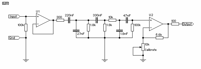
The purpose is supposedly to account for the fact that human hearing is less sensitive at low and high frequencies than in the upper midrange, and that this variation is dependent upon the sound intensity (SPL). The Fletcher-Munson curve...
The air-cored inductor L1 is constructed using 13 turns of 1mm diameter enamelled copper wire, featuring an inner diameter of 10mm. The completed inductor is positioned over R7, with its terminals soldered to those of the resistor. All electrolytic...
This project requires expensive hardware, including a microphone and amplifier, along with sophisticated audio analysis on the microcontroller. Even a complete microphone with an amplifier circuit does not yield the desired results, as noted in the product comments. The...