
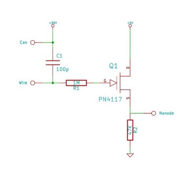
Static Electricity Detector

This circuit utilizes a Field Effect Transistor (FET) to achieve high input impedance, making it highly sensitive to small changes in voltage. The configuration involves leaving the gate terminal of the FET open, which allows it to detect minute variations in electric field strength. The use of a bare copper wire as a probe enhances the circuit's responsiveness to external electromagnetic influences.
To assemble the circuit, it is recommended to employ an open construction technique rather than using a printed circuit board (PCB) or veroboard. This approach minimizes parasitic capacitance and inductance that could otherwise affect the gate's performance and sensitivity. Components should be soldered together in a manner that maintains the integrity of the circuit's high impedance characteristics.
The probe, which is critical for the circuit's operation, should be handled with care. Direct contact with the probe can introduce unwanted noise or static discharge, which may compromise the circuit's accuracy. To mitigate this risk, it is advisable to insulate the probe within a non-conductive sleeve, such as a plastic pen casing. This insulation not only protects the probe but also helps to prevent interference from static electricity, which can carry either a positive or negative charge and affect the readings.
Overall, the circuit is designed for applications requiring high sensitivity to voltage changes, such as detecting static electricity or measuring weak electric fields. Proper construction and handling are essential to ensure accurate and reliable performance.This circuit relies upon the extra high input impedance of a FET, and also demonstrates the gate terminals sensitivity to changes in voltage. The gate terminal here is left open circuit, connected only to the "probe" this being just a few inches of bare copper wire.
With no fixed DC biasing, the gate terminal will respond to micro changes in voltage or "field strength". It is important not to make this circuit on veroboard or PCB material as this will reduce the effective gate impedance.
Instead use an "open" construction technique soldering each component together. The probe should not be touched directly and is best insulated in a plastic pen sleeve. As static electricity can have either a positive or nega 🔗 External reference
Related Circuits
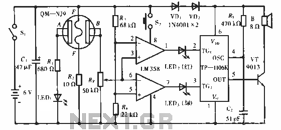
The QM-NJ9 is an alcohol sensor that detects the presence of alcohol by measuring the resistance values between points A and B. When alcohol is detected, the resistance decreases, leading to an increase in potential at point B. As...
The OpenRelief project is developing open, modular information solutions for disaster relief, which includes a range of network-enabled sensors. A radiation detector prototype has been created using an ionization chamber instead of a Geiger-Muller tube, constructed from an old...
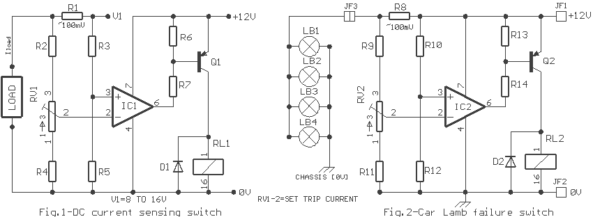
In Fig.1 see a DC current sensing switch, in which the current is applied from an 8 to 16 Volt supply. The R1 value is chosen so that it generates roughly 100 mV at the required trip current. In...
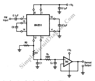
This is a linear frequency modulation (FM) detector circuit. This circuit is commonly utilized in telemetry applications and a wide range of analog communication systems. The primary component of this circuit... The linear FM detector circuit is designed to demodulate...
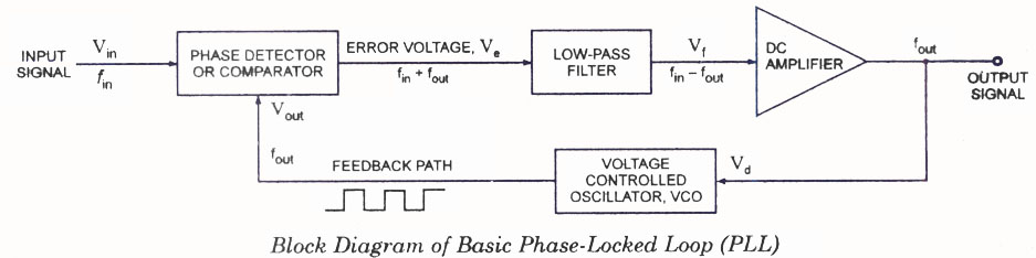
The operating principle of a Phase Locked Loop (PLL) is illustrated with a block diagram that includes a Phase Detector, Voltage Controlled Oscillator, and Low Pass Filter. A Phase Locked Loop (PLL) is an essential electronic circuit used in various...

A high-frequency audio signal (15 to 25 kHz) generated by Ul is fed to buffer Ql and SPKR1. A portion is fed to balanced mixer U2. Received audio picked up by SPKR2 (used as a microphone) is amplified by...