
Step-Down Charge Pump Regulator for USB Powered Devices
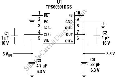
The step-down charge pump regulator is designed to efficiently convert a higher input voltage from USB sources (typically 5V) to a lower output voltage suitable for powering various electronic components. This type of regulator utilizes capacitors as energy storage elements and switches to control the flow of energy, enabling voltage reduction through a series of charge and discharge cycles.
Key components of the circuit include a switching control IC, capacitors, and diodes. The switching control IC manages the timing and operation of the switches, ensuring that the charge pump operates at the desired frequency for optimal efficiency. Capacitors are used to store and transfer charge, while diodes prevent reverse current flow, ensuring that the output voltage remains stable and within the specified limits.
The design must consider the physical area occupied by the components, as minimizing circuit area is crucial for integration into compact USB-powered devices. Careful selection of components, such as low-profile capacitors and integrated circuits, can significantly reduce the overall footprint of the circuit. Additionally, the layout of the PCB should be optimized to minimize parasitic inductance and capacitance, which can adversely affect performance.
Thermal management is also an essential aspect of the design. The charge pump's efficiency can lead to heat generation, particularly under load conditions. Proper heat dissipation techniques, such as using thermal vias and adequate copper planes, should be employed to ensure reliable operation.
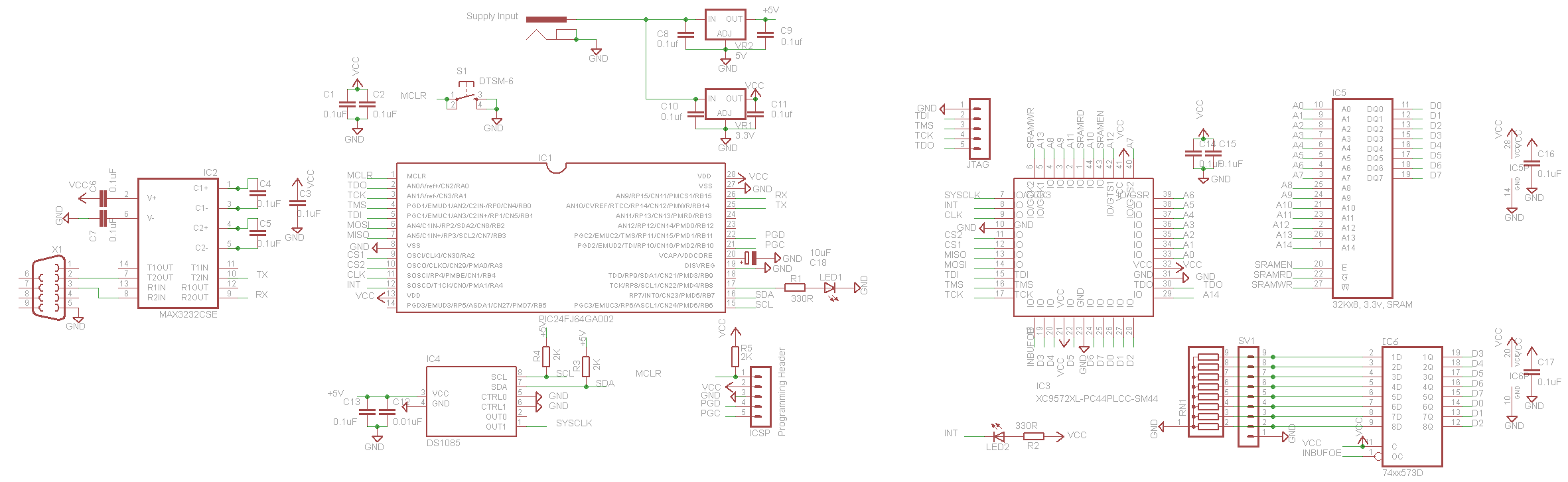
In summary, the step-down charge pump regulator circuit is a critical component for USB-powered devices, with its design focused on minimizing area while maintaining efficiency and thermal performance.this is a circuit of Step-Down Charge Pump Regulator for USB Powered Devices. The critical design parameter of this circuit is the circuit area. To solve this.. 🔗 External reference
Related Circuits
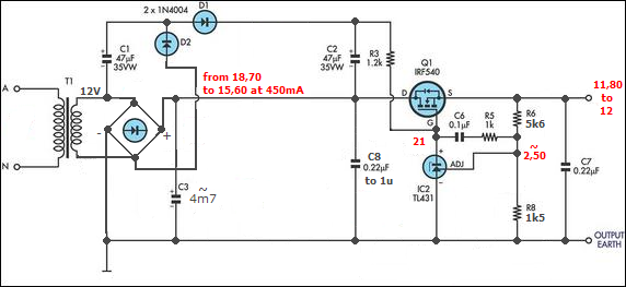
The half-linear design allows for reduced thermal considerations, as the linear regulator only needs to handle 1-5W instead of the full 75W per rail. MOSFETs operate in their linear region, just below the rated voltage for RDS(on), but they...

12V NiCad battery charger with a 200mA/h power supply. Refer to the specified page for an explanation regarding the related circuit diagram. The circuit for a 12V NiCad battery charger designed to supply a current of 200mA/h typically includes several...

Farmhand has read several pages and is attempting to understand more of the book. It can be challenging to comprehend at times how Tesla was able to achieve certain feats. The provided text reflects an individual's struggle to fully grasp...
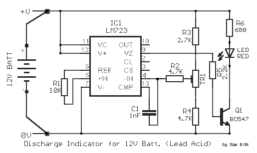
The circuit was designed to provide an indication before a 12 V lead-acid battery reaches a discharged state using an LM723 voltage regulator and a positive NPN standard voltage. The circuit utilizes the LM723 voltage regulator, which is well-suited for...
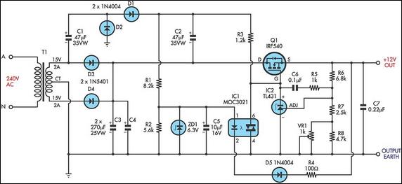
This circuit is a MOSFET-based linear voltage regulator with a voltage drop as low as 60 mV at 1 A. It utilizes a 15V-0-15V transformer and an IRF540 N-channel MOSFET (Q1) to provide a regulated 12V output. The gate...
Complex programmable logic devices (CPLDs) contain the building blocks for hundreds of 7400-series logic ICs. Complete circuits can be designed on a PC and then uploaded to a CPLD for instant implementation. CPLDs are integrated circuits that provide a versatile...