
Suitable for pager unit cell MAX1678 high-efficiency step-up power supply configuration
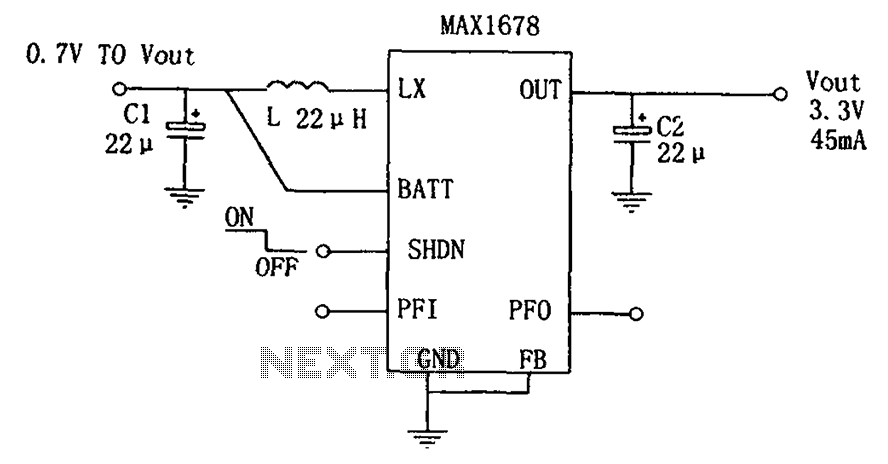
The MAX1678 integrated circuit is a highly efficient boost converter designed specifically for applications powered by low-voltage batteries. Its compact 8-pin package allows for easy integration into space-constrained designs, making it ideal for portable devices. The absence of external MOSFETs and Schottky diodes not only simplifies the circuit design but also enhances reliability and reduces manufacturing costs.
The battery voltage detection circuit is a critical feature that ensures the converter operates effectively within the specified input voltage range. This feature allows the circuit to automatically adjust its operation based on the battery voltage, providing a stable output even as the battery discharges. The noise suppression circuit further enhances performance by minimizing voltage ripple, which is essential for sensitive electronic applications.
The proprietary constant peak current control mechanism employed by the MAX1678 is a significant advancement over traditional PWM control methods. This technology enables the converter to maintain high efficiency across a wide range of loads while keeping quiescent current low, which is particularly beneficial in battery-powered applications where power conservation is paramount.
With an input voltage capability starting from as low as 0.7V, the MAX1678 is particularly versatile, allowing it to be used with a variety of battery types, including single alkaline or lithium cells. The preset output voltage of 3.3V is a standard level for many digital circuits, ensuring compatibility with a wide range of devices.
In summary, the MAX1678 boost converter is an ideal solution for low-power battery applications, providing high efficiency, compact design, and ease of use, making it suitable for a variety of portable electronic devices. Its advanced features and performance characteristics make it a valuable component in the design of modern electronic systems. As shown in FIG suitable for use in high-efficiency single pager battery power boost. It is composed of a MAX1678 and three external components. MAX1678 is designed for l to tw o battery-powered low-power applications and design. It uses ultra-small 8-pin, MAX package. No external MOSFET and Schottky diode, reducing the cost and size of the system cost. Chip with a battery voltage detection circuit, the noise suppression circuit. MAX1678 uses a proprietary constant peak current control principle, it is not only to maintain the traditional PWM converters low quiescent current, full load and with high efficiency and low output voltage ripple. It consists of a step-up switching power supply, can work in 0.7V input voltage, output voltage is preset at 3.3V.
Its characteristics are: efficiency above 90%; the input voltage is 0.85V to start; 45mA output current (1.2V to rise to 3.3V); quiescent current of 37 A, shutdown current 2 A; small, small external components, simple structure.
Related Circuits
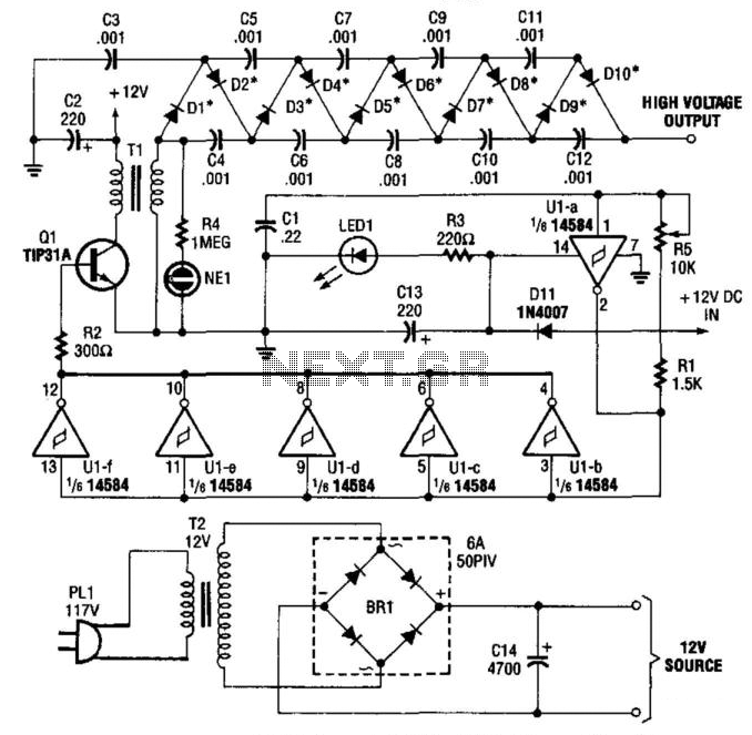
A CMOS oscillator (U1A) drives U1B through U1F, which in turn drives Q1, generating a 12-Vpp square wave across the primary of T1. This square wave is applied to a rectifier-multiplier circuit consisting of diodes D1 through D10 (each...
A Power Factor Correction (PFC) board has been obtained from an old Sun Microsystems Spark450 power supply (part number 300-1359-xx). This board contains all necessary components for a 650-watt inverter. However, the complete PFC circuit is not fully detailed...
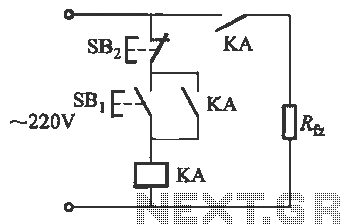
Power outages following a call prevent the re-closure of a circuit, which can help avoid the use of electrical appliances after the power grid is restored. If appliances are left on and a call occurs, it may lead to...
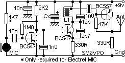
My FM Wireless Microphone has been a very popular project with beginners and experienced constructors alike. It has been used inside guitars and as the basis of a remote control system. I do however, receive many requests for a...
This is an RF Power Amplifier designed for low-cost QRP applications. The circuit operates over a broadband frequency range of 1.8 to 30 MHz, eliminating the need for tuning. The only adjustment required is to set the quiescent current...
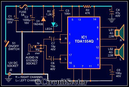
The circuit diagram illustrates a robust stereo amplifier capable of delivering 22W of power. It is based on the widely used single-chip audio power amplifier TDA1554Q (IC1), which is configured as two 22W stereo bridge amplifiers. While listening to...