
SW Receiver Using ZN414
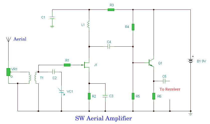
This circuit design effectively addresses the challenge of amplifying weak radio signals while minimizing noise interference through careful component selection and configuration. The use of a ferrite loop transformer enhances signal coupling, while the specific winding arrangement of the primary and secondary ensures optimal inductance for the desired frequency range. The tuning mechanism, achieved through a combination of fixed and variable capacitors, allows for precise adjustments to accommodate different signal frequencies, ensuring that the circuit remains versatile and adaptable to various applications.
The implementation of the 2N3819 FET in a common source configuration is critical for achieving the desired gain characteristics. The addition of a series resistor at the input helps to manage frequency response, preventing unwanted peaking that can occur due to the high Q factor of the choke in the drain circuit. The choice of a BC108C as a buffer ensures that the high output impedance of the FET does not adversely affect the subsequent stages of the circuit, allowing for improved signal integrity and stability.
Overall, this design exemplifies the principles of RF circuit design, balancing gain and noise performance while providing flexibility in tuning and component selection. Proper housing in a metal enclosure is recommended to mitigate external interference and enhance the reliability of the circuit in practical applications.The problem with amplifying weak radio signals is that you also amplify the noise. What you can receive depends on how much background noise is present, whether it be man made interference or static. In this design the RF signal is first met by a resistive attenuator, this is necessary as strong signals could otherwise overload your receiver.
The transformer T1 is would on a 1 inch diameter ferrite loop. The primary (antenna side) is 2 turns of 22 swg wire. The secondary is 4 turns of 22 swg wire. The 4 turns are spaced to occupy roughly half the coils circumference. The approximate inductance of the secondary is 20uH. To cover 5 to 20 Mhz a capacitor tuning from around 3pF to 200pF is required. A standard capacitor of 400 or 500pF (full mesh) can be used by including a series capacitor, C2 in the above Capacitors. Capacitors in series behave the same as resistors in parallel. The smallest capacitance is just less than the smallest capacitor in series and highest value also less than the highest capacitance.
With a 220pF capacitor for C2 and a 500pF variable capacitor (that tunes down to 5pF) the effective capacitance tunes 143pF to about 4. 8pF. This is roughly correct and not critical as the gain of the FET will amplify frequencies outside the tuned circuit range.
The 2N3819 FET operates in common source. The series base resistor R1 is included to even out the response, the internal gate source impedance is thus increased by R1 at higher frequencies. The drain circuit includes a 2. 5mH choke. A 4. 7mH can also be used. As the Q factor of these coils are high, a series resistor R3 is introduced to flatten the response. The frequency response is shown below calculated at 10% increments of VC1: The output impedance from the FET is high, so is buffered by the BC108C in emitter follower mode.
Current drain is around 3mA from a 9 Volt battery. As with any RF circuit, the circuit is sensitive to noise and interference. A metal or aluminum box would be a good choice for this project. However, on my trusty breadboard, this circuit preformed well, and weak signals were boosted well. 🔗 External reference
Related Circuits
For optimal efficiency, set MAX_STEPPERS to the number of stepper motors being controlled, with a maximum limit of four. Motors are identified by indices 0, 1, 2, and 3. On the QCard, there is a trade-off between the number...
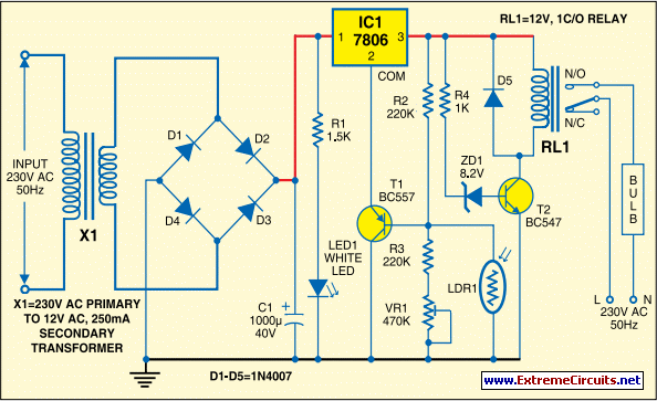
Voltage regulator ICs from the 78xx series deliver a stable output voltage in contrast to a highly variable input supply, provided that the common terminal is grounded. Any voltage applied above zero volts (ground) to the common terminal is...
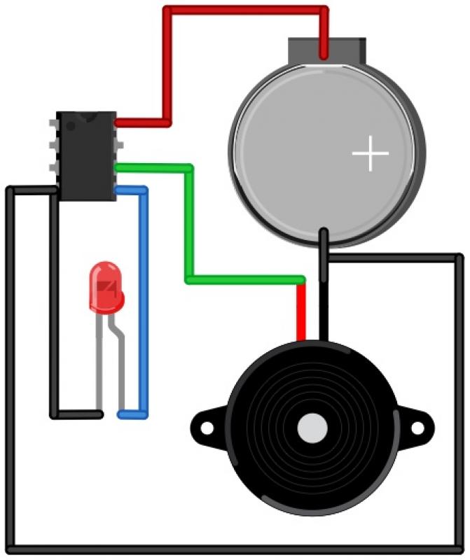
The Morse Beepy is a circuit designed to be simple and affordable, making it suitable for both children and adults as an introductory soldering project. It can be assembled and programmed within fifteen minutes to beep and blink a...
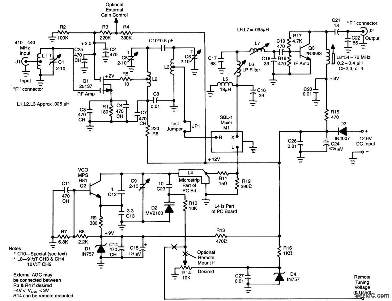
L1, Q1, L2, and L3 form an RF amplifier stage that drives M1, a doubly balanced mixer. Q4 serves as a local oscillator stage operating in the 375-MHz range. Signals in the 420 to 450-MHz range from Q1 are...
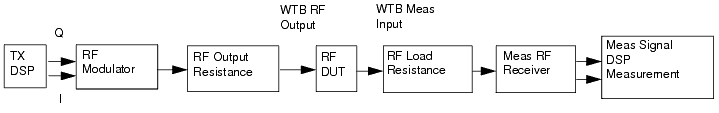
The 3GPPFDD_UE_RX is a test bench designed for testing the user equipment receiver in 3GPP FDD systems. It allows users to connect to an RF circuit device under test (DUT) and evaluate its performance through predefined measurements. This test...
Many audio systems consist of separate units, and due to economic reasons, only the amplifier is equipped with a remote control receiver module. In audio system designs where components are split into separate units, it is common for only the...