
Switching Improves Regulator Efficiency
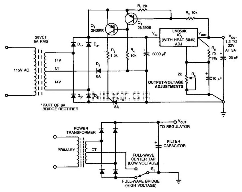
The circuit operates by utilizing a combination of a full-wave center tap (FWCT) rectifier and a full-wave bridge rectifier configuration to optimize the efficiency of the voltage regulation process. The central component, SCR D6, acts as a switch that toggles between these two configurations based on the voltage levels detected at the regulator output.
In the FWCT mode, with SCR D6 turned off, diodes D1, D2, and D5 conduct, allowing the circuit to convert the AC input voltage into a pulsating DC voltage. This configuration generates an output voltage of approximately 17 V, which includes a ripple component due to the nature of rectification. The pulsating DC voltage is fed into the voltage regulator, which is responsible for maintaining a stable output voltage.
The voltage drop across the regulator is critical as it provides the necessary base drive to transistor Q2. When Q2 is active (turned on), it prevents Q1 from conducting, effectively keeping SCR D6 off and maintaining the FWCT operation. This mode is efficient under normal load conditions, as it minimizes power dissipation within the regulator.
However, if the load demand increases and the output voltage of the regulator falls below a threshold of approximately 3 V, Q2 will deactivate. This action allows Q1 to turn on, which in turn activates SCR D6. Once D6 is on, the circuit transitions to the full-wave bridge configuration utilizing diodes D1 through D4. This configuration provides a more robust output by allowing current to flow through all four diodes, ensuring that the output voltage remains stable even under varying load conditions.
The switching mechanism between the two configurations enhances the circuit's overall efficiency and reliability. By dynamically adjusting the rectification method based on the output voltage, the design minimizes losses and optimizes performance across a range of operational scenarios. This approach is particularly beneficial in applications where maintaining a stable voltage is critical, such as in power supplies for sensitive electronic devices. In this circuit, a full-wave bridge is switched to a full-wave center tap to reduce regulator dissi pation. SCR D6 switches between configurations. When D6 is off, the circuit is an FWCT rectifier using Dl, D2, and D5. It applies 17 V plus ripple to the regulator input. The drop across the regulator supplies base drive to Q2. If Q2 is on, Ql is off, and D6 is off. If the regulator voltage drops below about 3 V, Q2 turns off, and turns Ql on, which turns on D6. This changes the circuit to an FW bridge using Dl through D4. 🔗 External reference
Related Circuits
MSP430 microcontroller and I2C-compatible slave peripheral device. Temperature measurement tasks can be accomplished in a variety of ways. The MSP430 microcontroller is a low-power, 16-bit device widely used in embedded systems, particularly for applications requiring efficient power management and precise...

This is a simple design for a voltage regulator circuit using a pass transistor. The design is built around the LM317T. The output current of the LM317T can be increased by incorporating an additional power transistor to share a...
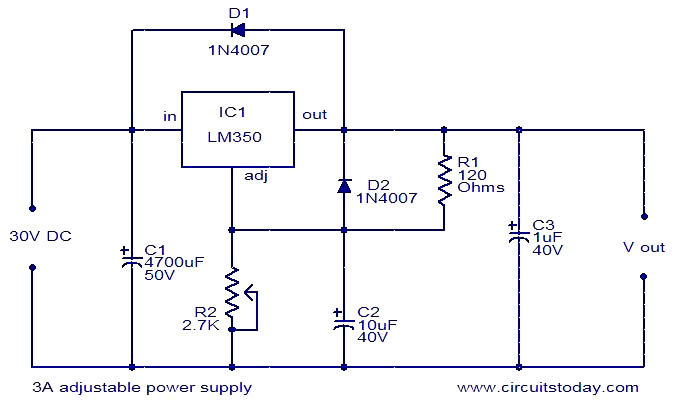
This circuit diagram illustrates a 3A adjustable power supply utilizing the LM350K integrated circuit. The LM350K is a robust voltage regulator IC that features thermal regulation and short circuit protection. The design adheres to application notes provided in the...
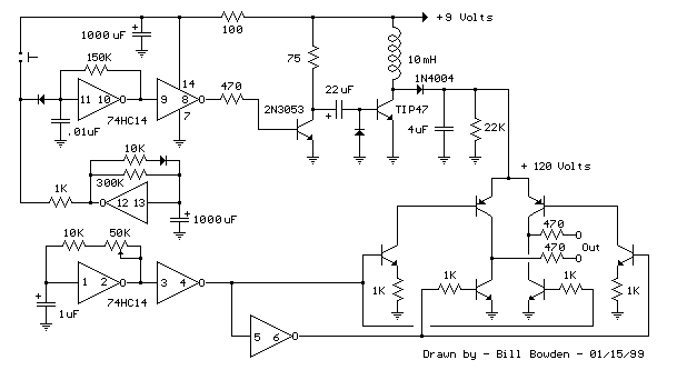
The telephone ring generator described generates the necessary aerial voltage using a simple switched-mode power supply (SMPS). It incorporates a CMOS Schmitt Trigger-based oscillator, a 10 mH inductor, a high-voltage switching transistor (such as the TIP47 or another high-voltage,...
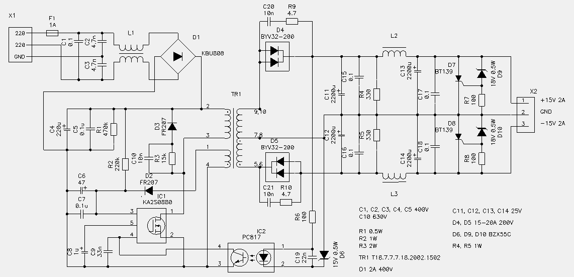
70 W switching power supply utilizing the KA2S0880 integrated circuit. Refer to the specified page for an explanation of the associated circuit diagram. The 70 W switching power supply designed with the KA2S0880 integrated circuit (IC) is a versatile solution...
An integrated voltage regulator connected in reverse to a mini drill allows for speed adjustment within specific limits, maintaining a constant speed regardless of load. The electronic speed control is achieved through a voltage regulator, which can power motors...