
switching loads with MOSFETs
Thermal power loss of the MOSFET device can be calculated as follows: 12.5A² * 40mΩ = 6.25W. The theoretical resulting device case temperature is 6.25W * 80 °K/W + 25 °C (ambient temperature) = 525 °C. This extreme temperature will certainly destroy the MOSFET. To prevent this, a heat spreader with at least 15 °K/W is recommended, which would yield a device temperature of approximately 120 °C at room temperature.
In a different scenario, the thermal power loss of the MOSFET device can also be calculated as 12.5A² * 10mΩ = 1.6W. The theoretical resulting device case temperature in this case is 1.6W * 40 °K/W + 25 °C (ambient temperature) = 90 °C.
The two diagrams in the top left illustrate a single switching sequence from the heat bed being off to on and back off. The leftmost diagram shows the voltage, while the adjacent diagram displays the drain current. It is evident that the highest voltages occur during the transition from the on state to the off state. The subsequent diagrams provide a zoomed-in view of the drain-source voltage (Vds) during this event. Notably, in the top rightmost diagram, a voltage of approximately 250V occurs at the drain of the IRF7936, which is rated for only 30V Vds. Although this overvoltage lasts only 100ns and may not immediately damage the device, prolonged exposure to such overvoltage can lead to device malfunction.
The leftmost three diagrams in the second row depict the Vds voltage for the PSMN7R0-60YS MOSFET used on RUMBA in various applications: heated bed, hotend with a 40W heater cartridge, and hotend with a Vishay heater resistor. The Vds voltage is approximately 68V, while the MOSFET (PSMN7R0-60YS) is rated only for 60V, indicating that it is also operating outside of its specifications. This situation is likely to cause eventual board malfunction.
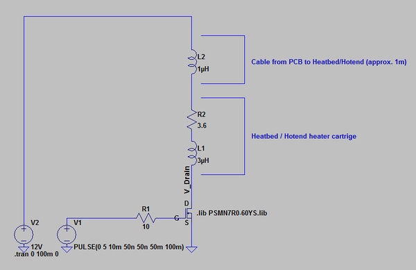
The circuit's favorable performance can be attributed to the inclusion of a freewheeling diode across the load (heat bed, hotend), which mitigates voltage overshoot. The schematic provided illustrates this simple circuit modification. It is crucial to check the RDS_on at Vgs=5V, as most devices are rated at Vgs=10V, leading to a significant difference in terms of RDS_on, which is considerably higher at Vgs=10V compared to 5V.
Utilizing a freewheeling diode across the load is essential, and the specifications for this diode are not particularly stringent. The current through this diode is less than 5A for approximately 0.5ms. A standard 1N4001 diode can suffice, as it can handle a forward current of 30A when the pulse duration is below 8ms.
In this application, the Vgs voltage is applied to the gate of the MOSFET, referenced to the source pin, which is connected to ground. The control voltage is sourced from the microcontroller output. Vds represents the voltage measured between the drain and source of the MOSFET, and it must not exceed the specified limit outlined in the datasheet. Typical voltage ratings for MOSFETs used in hotend and heatbed applications range between 20V and 60V.The biggest issue is that the RDS_on of the used MOSFETS is, driven with 5V gate voltage, too low. The other issue is that the the reverse voltage that occurs, when the MOSFET switches from on to off state kills the transistor. This revese voltage is caused by the parasitic series inductance of the heatbed, hotend heater cartride or resistor.
This article tries to generate understanding of what is happening. -> Thermal power loss of the MOSFET device: 12. 5A ² * 40mOhm = 6. 25W -> Theoretical resulting device case temperature 6. 25W * 80 °K/W + 25 °C (ambient temp. ) = 525 °C This definitely kills the MOSFET to survive add a heat spreader with at least 15 °K/W which results in a device temperature of approx. 120 °C at room temperature. -> Thermal power loss of the MOSFET device 12. 5A ² * 10mOhm = 1. 6W -> Theoretical resulting device case temperature 1. 6W * 40 °K/W + 25 °C (ambient temp. ) = 90 °C The two diagrams on the top left shows a single switching sequence from heatbed off - on - off The leftmost shows the voltage, the picture next to this the Drain current.
You can see that the highest voltages occur when switching from on state to off state. All other pictures show a zoomed view of the drain-source voltage (Vds) at this event. You can see that in the top rightmost diagram a voltage of approx. 250V(!) volts occures at the drain of the IRF7936. The device is rated only with 30V Vds. This voltage applys only 100ns and will not kill the device instantaneous but over time this overvoltage will lead to malfunction of the device. The leftmost three diagrams in the second row show the Vds voltage for the PSMN7R0-60YS MOSFET used on RUMBA in different applications: Heated bed, Hotend with 40W heater cartrige and Hotend with Vishay heater resistor.
As you can see the Vds voltage is approx. 68V. The MOSFET device (PSMN7R0-60YS) is only rated at 60V. This is also out of the specification of the device. Sooner or later it will result in malfunction of the board. What is the reason for this excellent behaviour The circuit is using a freewheeling diode across the load (heatbed, hotend) which prevents the voltage overshoot. The schematics below shows the (simple) circuit change. Always look for the RDS_on @ Vgs=5V most Devices are specified at Vgs=10V this makes a big difference in terms of RDS_on which is in this case (Vgs=10V) significantly higer at 5V Vgs.
Use a freewheeling diode across the load. The requirements on that diode are not very high. The current through this diode is < 5A for approx. 0. 5ms. For example a simple 1N4001 diode can make the job. Its allowed forward currend is 30A(!) when the pulse time is below 8ms. Vgs voltage applied to the gate of the MOSFET referenced to the source pin. In our application the source pin is tied to GND(ground). This is the control vopltage coming from the µController output Vds is the votage measured between drain and source of the MOSFET. This voltage must not be higher than specified in the datasheet. Typical values for MOSFETs used for hotend and heatbed are between 20. 60V 🔗 External reference
Related Circuits

The triac will be activated at the beginning of the positive half cycle due to the current flowing through the 3 µF capacitor, provided that the C103 SCR is in the off state. The load voltage subsequently charges the...

The silicon carbide (SiC) MOSFET offers notable advantages, including a straightforward drive circuit. It possesses unique characteristics that render it a superior switching device in comparison to traditional options. The silicon carbide MOSFET is a type of field-effect transistor that...
A 15 Watt switching power supply schematic diagram features a pulse transformer T1 constructed on a ferrite core M2500NMS-2 or M2000NM9, with a Sh5h5 size (cross-section of the magnetic coils at the location of 5G—5 mm with a gap...
A switching power supply with an output voltage significantly lower than its input voltage exhibits an interesting characteristic: the current drawn by the supply is less than its output current. However, the input power (UI) is greater than the...

If a negative supply is required for an operational amplifier or if a negative bias voltage is needed while operating from a single supply voltage, such as in battery applications. To generate a negative supply voltage from a single positive...

In broadband networking and high-speed computing applications, multiple high-current, low-voltage power supplies are required to power FPGAs, flash memory, DSPs, and microprocessors. One example specifies a maximum current of 60A to power the CPU at 1.5V and up to...
Warning: include(partials/cookie-banner.php): Failed to open stream: Permission denied in /var/www/html/nextgr/view-circuit.php on line 713
Warning: include(): Failed opening 'partials/cookie-banner.php' for inclusion (include_path='.:/usr/share/php') in /var/www/html/nextgr/view-circuit.php on line 713