
Synchronous Camera Flash Trigger Using IGBT

The circuit operates by utilizing a comparator to detect the primary flash and subsequently trigger the secondary flash via the IGBT. The LM339 comparator is chosen for its low input offset voltage, which enhances the accuracy of the triggering process. The circuit design includes a resistor divider network that sets the reference voltage at the inverting input, ensuring that it remains stable during operation.
When the primary flash occurs, the light sensor (CdS, photodiode, or phototransistor) detects the light intensity, leading to a rapid decrease in resistance. This change in resistance results in an increase in voltage at the non-inverting input of the comparator. Once this voltage exceeds the reference voltage, the comparator output switches to a high state, activating the gate of the IGBT.
The Toshiba GT8G131 IGBT is selected for its high-speed switching capabilities and robustness under high current conditions, making it ideal for flash applications. It is essential to ensure that the gate voltage applied to the IGBT is adequate to fully turn it on; typically, this voltage should be around 10-15 volts for optimal performance. If the voltage is too low, the IGBT may not enter the saturation region, resulting in insufficient current flow to trigger the flash tube effectively.
In summary, this circuit provides a reliable and efficient method for triggering a secondary camera flash, utilizing the advantages of IGBT technology while ensuring compatibility with various light sensors and camera models. Proper attention to the gate voltage and component selection is crucial for the successful operation of this flash triggering circuit.Typically a synchronous camera flash (e. g. slave flash) is triggered via an SCR. In this blog post, I will show you a circuit that can be used to trigger a secondary camera flash using an IGBT. Using an IGBT for camera flash triggering has several advantages over the traditional SCR triggering mechanism: for instance, the width of the triggering pulse can
be controlled precisely and thus enabling functions such as red eye prevention that cannot be achieved easily using an SCR triggered circuit. Depending on the camera used, the light sensor can be either a CdS photoresistor, a photodiode or a phototransistor.
For many automatic cameras, a photodiode or photo transistor maybe necessary as the shutter speed is typically faster than then reaction time of a CdS sensor. The schematics above also shows how both types of sensors can be used. Here is how this circuit works. The inverting input of the comparator (LM339) is referenced at roughly Vcc/2. When the CdS sensor detects the primary camera flash, its resistance drops and the voltage at the none-inverting input exceeds the reference voltage.
The comparator output a high (e. g. close to Vcc) and thus triggers the IGBT. The IGBT used here is a Toshiba GT8G131 N Channel IGBT, which is specifically designed for strobe flash applications. It is important to supply a high enough (within safety limit) gate voltage to ensure that the IGBT is fully turned on.
Otherwise, the IGBT may not be able to conduct a high enough current to trigger the flash tube. So if you are using other types of IGBT, you may need to adjust the Vcc accordingly. 🔗 External reference
Related Circuits

The TDA 7294 from T-MICROELECTRONICS is a monolithic integrated circuit housed in a "Multiwatt 15" package, primarily designed for use in Class AB amplifiers for high-fidelity applications, including stereo systems, active speakers, and television receivers. Its large feed area...
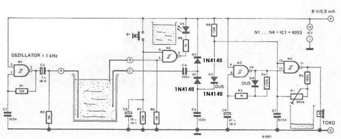
The circuit diagram is straightforward and operates as follows: the N1 Schmitt trigger functions as an oscillator, producing a frequency of approximately 1 kHz. When there is sufficient water in the tank, alternating voltage flows from electrode A to...
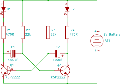
A two-transistor circuit that alternately flashes two LEDs on and off. This tutorial demonstrates how beginners in electronics can build this simple circuit on a breadboard. This circuit utilizes two NPN transistors configured in a flip-flop arrangement, which allows for...

The UTC7642 is designed for use in low voltage portable radio cassette systems and other wireless AM systems. It is packaged in a TO-92 casing. The manufacturer is LianShun Electronics Co., Ltd. The UTC7642 is a low-voltage operational amplifier...
Audio Amplifier with output power of either 100W or 130W. The output configuration can accommodate 2 transistors for 90W output or 4 transistors for 130W output. The PCB layout utilizes T3 on the heatsink. The component reference and values...

The schematic consists of four hardware blocks: 1) The wall transformer 2) The charging circuit 3) The control unit 4) The output stage. The circuit schematic is structured around four essential hardware blocks that facilitate the overall functionality of the...
Warning: include(partials/cookie-banner.php): Failed to open stream: Permission denied in /var/www/html/nextgr/view-circuit.php on line 713
Warning: include(): Failed opening 'partials/cookie-banner.php' for inclusion (include_path='.:/usr/share/php') in /var/www/html/nextgr/view-circuit.php on line 713