
Synchronous Counters
A synchronous binary counter is a fundamental digital circuit used in various applications such as frequency division, digital clocks, and event counting. The design involves the interconnection of flip-flops and combinational logic gates to achieve the desired counting sequence. The counter's operation is dictated by a clock signal, which synchronously triggers the state changes of the flip-flops.
In a typical implementation, each flip-flop is configured in a toggle mode, responding to the clock pulses. The first flip-flop toggles on every clock pulse, while subsequent flip-flops change their state based on the outputs of lower-order flip-flops. This cascading effect creates a binary counting sequence. The use of AND gates to determine when to toggle higher-order flip-flops is crucial for maintaining the synchronous nature of the counter.
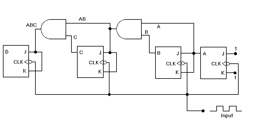
To visualize this, consider a 4-bit synchronous up-counter. It consists of four flip-flops (FF0, FF1, FF2, FF3) and three AND gates. The output of FF0 feeds directly to the clock input of FF1, while the outputs of FF0 and FF1 are combined in an AND gate to control the clock input of FF2. Similarly, the outputs of FF0, FF1, and FF2 are fed into another AND gate to control FF3. This arrangement ensures that all flip-flops toggle simultaneously when the conditions are met.
The propagation delay through the AND gates can impact the overall speed of the counter. To mitigate this, designers may implement techniques such as hierarchical structuring, where groups of flip-flops are managed separately to reduce fan-out and propagation delay. This approach allows for efficient resource utilization while maintaining the synchronous operation of the counter.
In summary, the design of synchronous binary counters is a complex yet rewarding endeavor that combines the principles of digital logic and Boolean algebra. The understanding of flip-flops, propagation delays, and combinational logic is essential for creating efficient counting circuits that can be utilized in a wide range of electronic applications.The material is presented in a manner suitable for a teaching tool. It seeks to enlighten and to spark off interest in the design of counters. As R. S. S Obermann remarks ". design of counters has, in my experience, always been an excellent proving ground for anyone who has mastered Boolean algebra. Have fun reading ! A synchronous binary counter counts from 0 to 2N-1, where N is the number of bits/flip-flops in the counter. Each flip-flop is used to represent one bit. The flip-flop in the lowest-order position is complemented/toggled with every clock pulse and a flip-flop in any other position is complemented on the next clock pulse provided all the bits in the lower-order positions are equal to 1. Take for example A4 A3 A2 A1 = 0011. On the next count, A4 A3 A2 A1 = 0100. A1, the lowest-order bit, is always complemented. A2 is complemented because all the lower-order positions (A1 only in this case) are 1`s. A3 is also complemented because all the lower-order positions, A2 and A1 are 1`s. But A4 is not complemented the lower-order positions, A3 A2 A1 = 011, do not give an all 1 condition.
To implment a synchronous counter, we need a flip-flop for every bit and an AND gate for every bit except the first and the last bit. The diagram below shows the implementation of a 4-bit synchronous up-counter. From the diagram above, we can see that although the counter is synchronous and is supposed to change simultaneously, we have a propagation delay through the AND gates which add up to give an overall propagation delay which is proportional to the number of bits of the counter.
To overcome this problem, we can feed the outputs from the flip-flops directly to a many-input AND gate as follows : This method does overcomes the problem of additive propagation delay but introduces some other problem of its own. From the diagram above, we can see that the third flip-flop gets its J-K input from the output of a 2-input AND gate and the fourth flip-flop gets its input from a 3-input AND gate and so on.
If we have a counter that counts to for example 16 bits, we will need to have : This method obviously usus a lot more resources than the first method. Not only that, in the first method, the output from each flip-flop is only used as an input to one AND gate.
In the second method, the output from each flip-flop is used as an input to all the higher-order bits. If we have a 12-bit counter, the output of the first flip-flop will have to drive 10 gates (called fan-out.
The output from the flip-flop may not have the power to do this. The "solution" to this is to use a compromise between the two methods. Say we have a 12-bit counter, we can organise it into 3 groups of 4. Within each group of 4, we use the second method and between the 3 groups, use the first method. This way, we only have an overall gate propagation delay and a maximum fan-out of 3 instead of 10 using the first and second method respectively. There are many variations to the basic binary counter. The one described above is the binary up counter (counts upwards). Besides the up counter, there is the binary down counter, the binary up/down counter, binary-coded-decimal (BCD) counter etc.
Any counter that counts in binary is called a binary counter. In a binary up counter, a particular bit, except for the first bit, toggles if all the lower-order bits are 1`s. The opposite is true for binary down counters. That is, a particular bit toggles if all the lower-order bits are 0`s and the first bit toggles on every pulse.
Taking an example, A4 A3 A2 A1 = 0100. On the next count, A4 A3 A2 A1 = 0011. A1, the lowest-order bit, is always complemented. A2 is complemented because all the lower-order positions (A1 only in this case) are 0`s. A3 is also complemented because all the lower-order positions, A2 and A1 are 0`s. But A4 is not complemented the lower-order positions, A3 A2 A1 = 011, do not give an all 0 condition. The implemen 🔗 External reference
Related Circuits
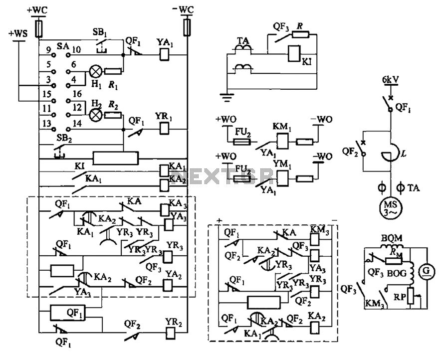
The circuit depicted in Figure 3-189 includes various components such as switch SA, closing button SBi, trip button SBz, de-excitation switch Yaa, and off trip coil YR3. The excitation switch contacts are represented by QF3, which serves as a...
Modern exhibitions utilize extensive sound, light, and electrical technologies for advertising, promotion, and propaganda. This involves various electrical diagrams and control models. Commonly used is an automatic program circuit with pre-recorded commentary, which requires synchronization of two mating times....
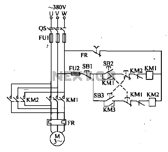
The forward and reverse dual interlock control circuit is based on the control circuit depicted in Figure 4-4, with an enhancement that incorporates a composite mechanical button interlock. The advantage of this circuit is that it allows the motor...
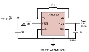
The LTC3525-3/LTC3525-3.3/LTC3525-5 are high-efficiency synchronous step-up DC/DC converters with output disconnect capability that can operate with an input voltage as low as 1V. These converters provide a compact and efficient alternative to charge pumps for single-cell or dual-cell alkaline...
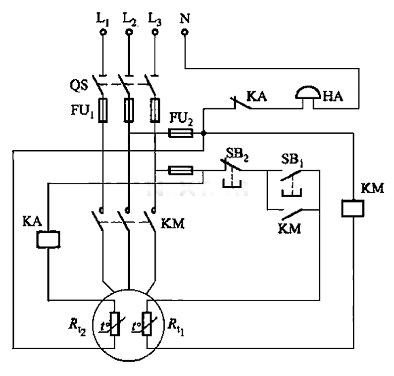
The circuit illustrated in Figure 4-2 employs two thermal resistors. One, designated as Rc, functions as overload protection, while the other, labeled Rt, serves as an alarm. The circuit in question integrates two thermal resistors to monitor temperature changes and...
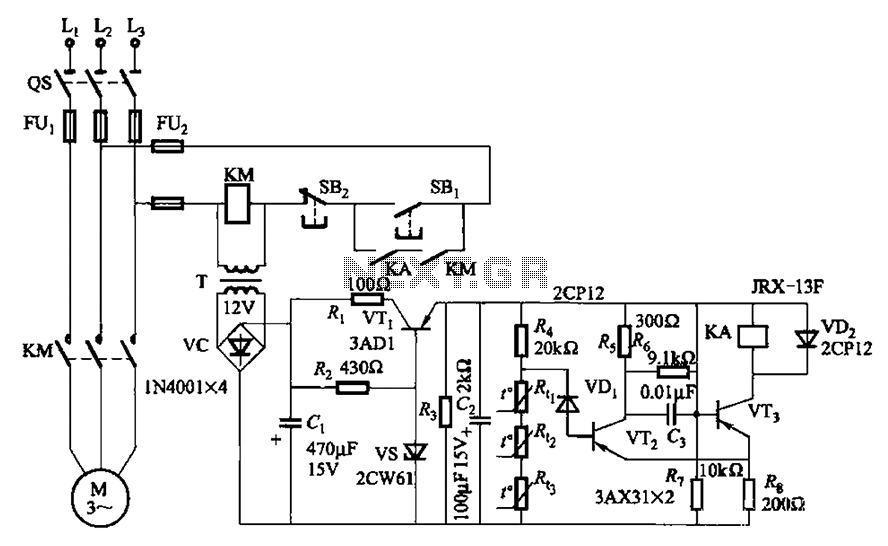
A P-type transistor (VT2, VT3) and other components form a common emitter-coupled trigger, functioning as a Schmitt trigger device. This setup serves as a switching circuit to detect changes in the resistance of a PTC thermistor, thereby controlling the...