
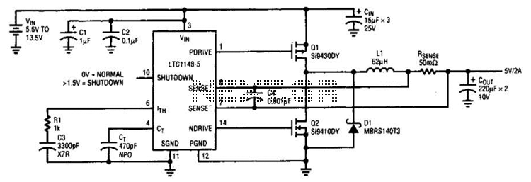
Synchronous Stepdown Switching Regulator Circuit
The benefits of current control include superior line and load transient rejection, built-in short-circuit protection, and regulated startup currents. The peak inductor current is limited to 150 mV/SENSE or 3 A for the circuit described in A.
The LTC 1148 is a high-efficiency DC-DC converter designed for surface-mount applications. It is capable of delivering a regulated output voltage of 5 V at a maximum load current of 2 A, making it suitable for various electronic devices requiring stable power supply. The input voltage range of 5.5 V to 13.5 V allows for flexibility in power source selection, accommodating a wide array of applications.
The efficiency of the LTC 1148 is a critical parameter, with a peak performance of 97% and maintaining over 90% efficiency across a load range from 10 mA to 2 A when supplied with a 10 V input. This efficiency is essential for minimizing heat generation and maximizing battery life in portable applications.
The circuit employs two key components: Q1, the main switch, and Q2, the synchronous switch. These transistors work in tandem to regulate the output voltage by rapidly switching on and off in response to the load conditions. The inductor current is monitored through a current shunt, which provides a voltage drop proportional to the current flowing through it. This measurement is critical for feedback control, ensuring that the output voltage remains stable under varying load conditions.
The /vgENSE component plays a vital role in defining the output current capability. The formula QOUT = 100 mV/ftSENSE indicates that the output current can be accurately set by adjusting the voltage across the sense resistor, allowing for precise control over the power delivered to the load.
Incorporating current control into the design offers significant advantages, including excellent transient response to sudden changes in load or input voltage, which is critical for maintaining stable operation in dynamic environments. Additionally, the built-in short-circuit protection enhances the reliability of the device, preventing damage during fault conditions. Controlled startup currents further contribute to the safety and longevity of the circuit by mitigating inrush current effects that could adversely affect other components in the system.
The circuit limits peak inductor current to 150 mV/SENSE, translating to a maximum of 3 A, which protects the converter from excessive current that could lead to overheating or failure. This design consideration is crucial for maintaining the integrity and performance of the LTC 1148 in various applications. A shows a typical LTC 1148 surface-mount, application providing 5 V at 2 A from an input voltage of 5.5 V to 13.5 V. The operating efficiency, shown in B, peaks at 97% and exceeds 90% from 10 mA to 2 A with a 10-V input.
Ql and Q2 comprise the main switch and synchronous switch, respectively, and inductor current is measured via the voltage drop across the current shunt. /vgENSE is the key component used to set the output, current capability according to the formula/QUT =100 mV/ftSENSE.
The advantages of current control include excellent line and load transient rejection, inherent short-circuit protection and controlled startup currents. Peak inductor current is limited to 150 mV//SENSE or 3 A for the circuit in A. 🔗 External reference
Related Circuits
Can someone please help explain how this circuit works? I am confident that I understand how the voltage divider network operates. The circuit in question likely includes a voltage divider configuration, which is a fundamental concept in electronics used to...
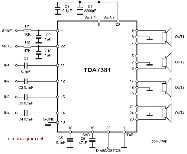
The amplifier is a quad amplifier circuit (amplifier with four inputs and four outputs) based on the TDA7381. This amplifier is designed for car audio systems, but it can also be utilized for other applications. The circuit has a...
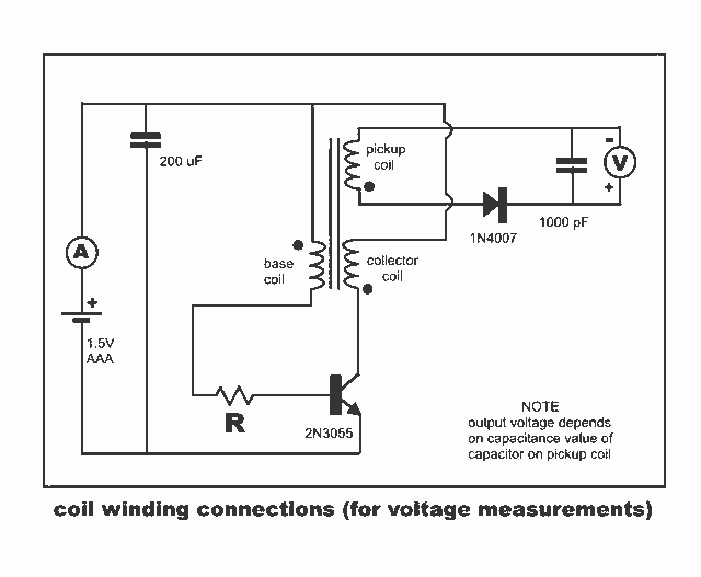
New Jewel Thief "Resonate LCR Circuit" with significantly reduced energy consumption. Measurements of voltage and current for the Joule thief. The Jewel Thief circuit, particularly the "Resonate LCR Circuit," is an innovative low-power design that enhances energy efficiency while maintaining...
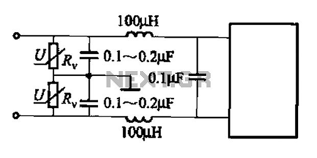
A common low-pass filter circuit is illustrated. Figures (a) to (c) demonstrate its ability to suppress high-frequency interference, while Figure (b) shows a varistor that can absorb lightning surge voltage. Figure (d) indicates the circuit's capability to suppress low...
In conventional applications, switching-regulator integrated circuits (ICs) regulate the output voltage (VQVT) by controlling the current through an external inductor. However, the IC in configuration A utilizes a diode-capacitor network in place of the inductor, providing comparable performance for...
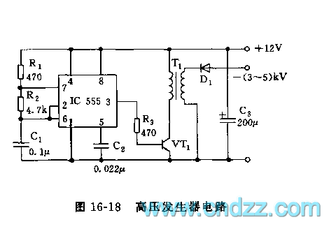
The high voltage generator depicted in figure 16-18 utilizes the 555 timer IC as its primary component. The oscillating voltage produced is enhanced through a step-up transformer. The astable multivibrator configuration comprises the 555 timer along with resistors R1...