
TDA6103Q having a feedback factor of the test circuit
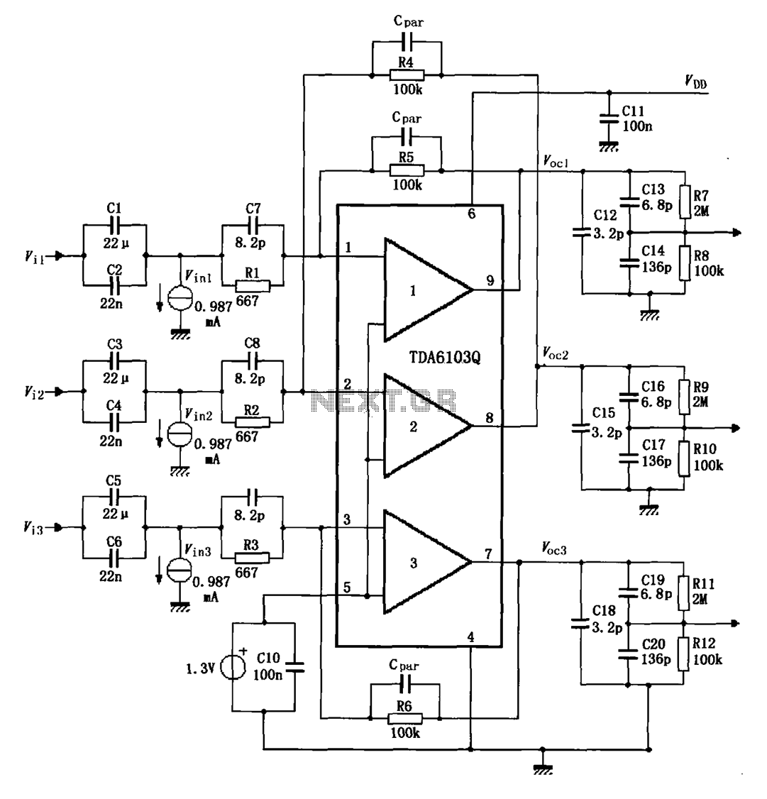
The TDA6103Q is a versatile integrated circuit primarily used in video signal processing applications. In this configuration, the circuit is designed to amplify input signals while maintaining a stable feedback mechanism to ensure optimal performance. The feedback factor of 1/150 indicates that the circuit is set to provide a moderate level of gain, suitable for various signal conditions.
The input resistor network serves to condition the incoming signals Vi1, Vi2, and Vi3, which may originate from different sources such as video cameras or other video processing units. The capacitors in this network filter high-frequency noise, allowing only the desired signal frequencies to pass through to the differential inputs of the TDA6103Q. Pins 1, 2, and 3 are crucial as they define the differential input stage, where the circuit compares the inverting and non-inverting inputs to generate the amplified output.
The output network, composed of resistors R2 and R3 and capacitors Cn, C8, and C9, is responsible for shaping the output signal and ensuring that it meets the required specifications for further processing or display. The arrangement of these components can influence the bandwidth and frequency response of the output signal, allowing for fine-tuning based on application needs.
The feedback network, which includes resistors R4, R5, and R6 in conjunction with the capacitor Cpar, plays a critical role in stabilizing the output signal. By providing feedback from the output to the input, these components help to regulate the gain and maintain the desired signal integrity. The configuration ensures that variations in input signal levels do not adversely affect the output, thus achieving automatic black level stabilization. This feature is particularly important in video applications, where consistent brightness and contrast levels are essential for high-quality image reproduction.
Overall, the TDA6103Q test circuit is a well-structured design that effectively manages video signal amplification and stabilization, making it suitable for various electronic applications in the field of video processing.As shown in FIG TDA6103Q test circuit with feedback factor is 1/150. Input signal Vi1, Vi2, Vi3 through the input resistor network consists of capacitors into the TDA6103Q 1,2,3 feet, 2, 3 feet and 5 feet are inside the differential input stage of the inverting input terminal and inverting input terminal. The amplified signal from 9,8,7 feet respectively output through the output network of R2, R3, Cn, C8, C9 composed of between 1 to probe to the probe pin 3.1,9 resistor R5 in parallel with the capacitor Cpar composition feedback network; 2,8 feet between the resistor R4 in parallel with the capacitor Cpar feedback network consisting; 3,7 feet between the resistor R6 and the capacitor connected in parallel Cpar feedback network from the current automatic black level stabilizing role.
Related Circuits
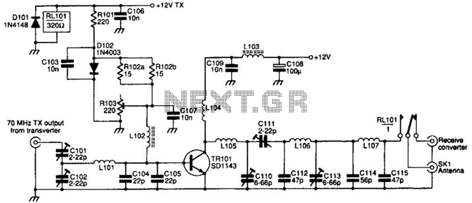
The SD1143 transistor offers a gain of approximately 14 dB in this circuit. Its design takes advantage of the fact that a 175-MHz device exhibits significantly higher gain when operated at lower frequencies. The amplifier was initially intended for...
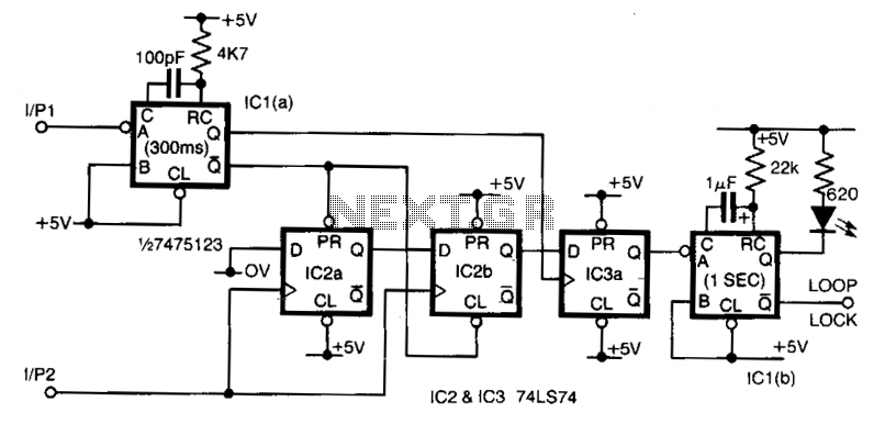
Input 1 functions as a gating period, during which a single rising edge on input 2 produces a logic 1 output. Any other input that indicates non-identical frequencies results in a logic 0 output. IC1a converts input 1 into...
In electronic technology, the triode utilizes a variety of general components and parts. The parameters of the triode and numerous electrical parametric measurement schemes are closely related to measurement results. Therefore, in electronic design, the base pin, typological judgment,...
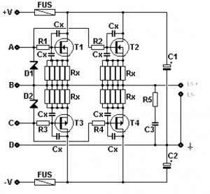
Amplifier circuit featuring a MOSFET output stage, serving as an alternative to the output stage that utilizes bipolar transistors. Advantages of the MOSFET amplifier include ease of operation, the ability to handle hundreds of watts with straightforward parallel configurations,...

None of this triggering circuitry is exactly what is desired, but it will provide a starting point in the right direction. The triggering circuitry mentioned serves as a foundational element for various electronic applications, particularly in the realm of signal...
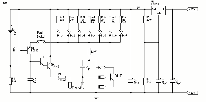
The design objective was to produce an hFE tester with switched collector currents for the DUT (Device Under Test) covering a range suitable for the selection and matching of output transistors for amplifiers such as the JLH Class-A, ESP...
Warning: include(partials/cookie-banner.php): Failed to open stream: Permission denied in /var/www/html/nextgr/view-circuit.php on line 713
Warning: include(): Failed opening 'partials/cookie-banner.php' for inclusion (include_path='.:/usr/share/php') in /var/www/html/nextgr/view-circuit.php on line 713