
telephone ring generator circuit

The circuit operates by first converting the AC mains to a lower voltage using a transformer, followed by rectification and filtration to obtain a stable DC supply. The clock generation circuitry, utilizing a Schmitt trigger and flip-flops, ensures a reliable timing signal for the EPROM, which holds the ringing sequences. The gating mechanism controlled by the NAND gate and VMOS FET allows for efficient switching of the ringing signal, ensuring minimal power loss and enhancing performance. The choice of components, such as the VMOS FET for its low on-resistance and built-in protection, reflects a design focused on reliability and efficiency. The system's modularity allows for various ringing sequences to be programmed into the EPROM, making it adaptable for different applications. The use of salvaged components not only reduces costs but also promotes sustainability in electronic design. This circuit exemplifies a practical approach to creating a customizable ringing device with modern electronic components and techniques.This is a switch selectable dual output "re-hashed" version of my previous (2007) design, and uses a field programmed EPROM for generating both versions of the ringing sequence. AC mains is stepped down to about 10 v AC and fed to the familiar bridge rectifier, filter capacitor and 3 terminal voltage regulator.
However a series diode is inserted b etween the + terminal of the bridge rectifier and the filter capacitor. Therefore at the anode end of this diode will be a pulsating 100Hz unidirectional sinusoid which is used as an accurate "clock" (Cathode end being filtered DC voltage) This positive going sinusoid is fed to a 4093 Schmitt trigger, its action produces a fast rise (and fall) square wave output necessary to clock following logic IC`s. A clamping diode b/w the Schmitt input (pin 2) and the Vcc rail precludes the input from rising greater than one diode drop above Vcc, excess voltage being dropped across 1K resistor.
It was found by experiment that a 22K "bleed" resistor was needed at the gate input to prevent "lock-up" due to some sort of "charge storage" effect. This cleaned-up 100Hz "clock" signal is now fed to a 4013 D type flip-flop which divides the signal by 2 and also gives a 50 Hz equi` mark/space signal.
This then feeds the 7490 where another divide by 2 gives; 25Hz (for ringing frequency) and further divide by 5 give 5Hz or a 200mS interval suitable for producing the correct ring cadence. The sequential outputs of the 4040 are connected to the address lines of a 2716 eprom which has been field programmed to provide a serial output bit-stream of 200mS interval used as a gating signal to enable on and off the 25Hz ringing signal.
For each 200mS clock pulse the output of the eprom moves to the next sequential address. The first 64 locations contain the necessary coding for two runs of the UK sequence and the next 64 memory addresses`s contain coding for the 4 sec ring, 8 sec silence US sequence. However the astute reader will realise that many other types would work, and in fact we are only using 128 address locations and one bit of the 8 bit wide data byte stored in the eprom (D0) The eprom contents are shown in the table (below) it can be seen that the pink higlighted locations represent a "ring" and all others silence (read from top to bottom) Gating is achieved in the 4093 NAND gate, its output then inverted directly feeds a VMOS FET gate which switches the unregulated 15v rail onto the transformer primary.
The VMOS FET is preferred over a bipolar transistor etc here because of their power handling capacity and very low "on" state resistance (milliohms) which allows most of the +15v DC rail be available to the transformer winding. Fortunately these devices also have an internal reversed biased diode, b/w drain and source which protects them against failure from transient spikes (refer to manuf` data sheets).
The particular FET specified 2SK3296, I salvaged several from defunct P4 computer mother board (in power supply circuit). However suitable replacement types are easily available. I have used a 5000 ohm to 4 ohm loud-speaker transformer (in reverse - so to speak) to step up the voltage to the level necessary the make the bell solenoid actuate the armature (1 : 35 ratio) Simply remove the internals (circuit board, fan etc) and you have a 6" x 6" x 3" sized metal box with IEC entry connector and on/off mains switch etc - ready for re-use.
🔗 External reference
Related Circuits
A small audio test generator is very useful for quickly tracing a signal through an audio unit. Its main purpose is speed rather than refinement. An audio test generator is an essential tool in the field of audio engineering, primarily...
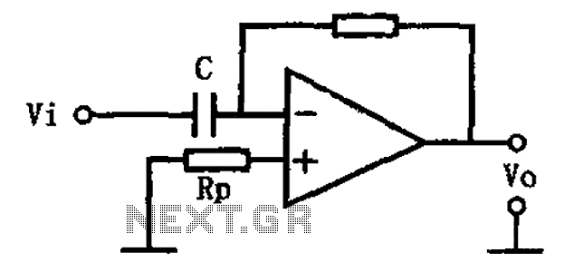
This circuit illustrates a basic differentiating circuit. The differential operation circuit can process input and output signals, establishing a relationship between the output and the input. A basic differentiating circuit is designed to produce an output that is proportional to...

Traditional control methods for fan power equipment involve manual or relay control, which often leads to issues of poor reliability and flexibility. For instance, when the motor capacity is large, the startup process can be prolonged, resulting in high...
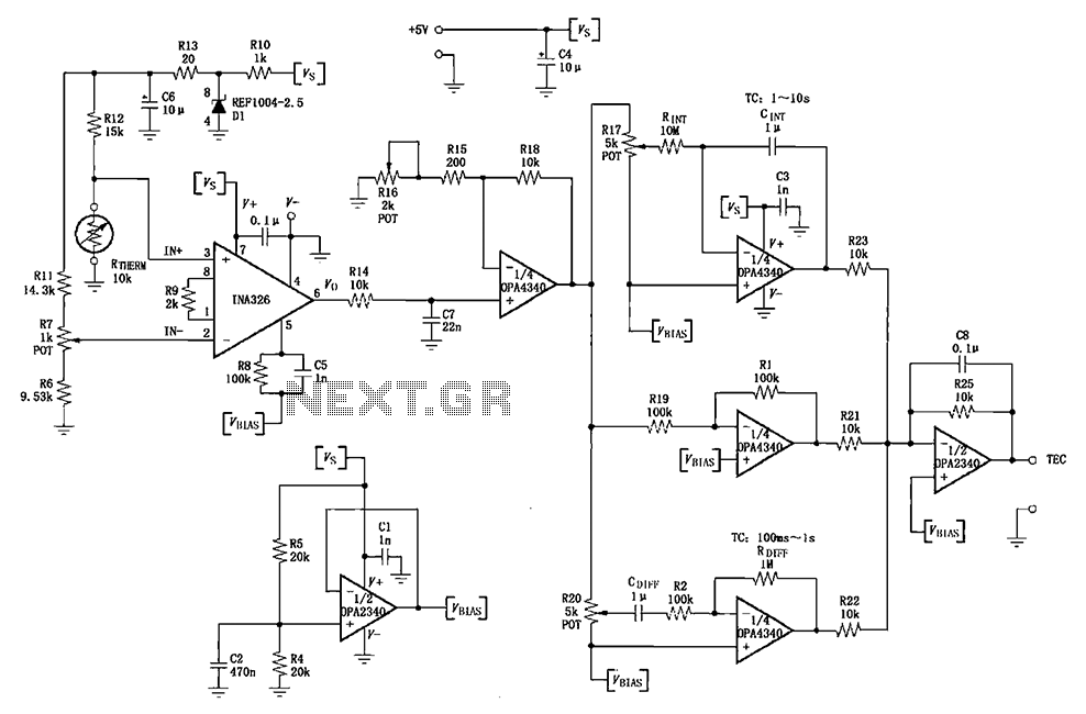
The INA326/327 forms a single power PID (proportional-integral-derivative) controller as illustrated in the temperature control loop. This circuit is primarily designed for temperature measurement and control. A thermistor, designated as RTHERM, detects temperature changes and converts them into an...
After being careful about every orientation of every transistor, a circuit board was designed around the LM387N, which was not the intended chip nor the one originally ordered (LM258, commonly referred to as LM358). During testing before adding larger...
A peak detector is a circuit that detects the peak voltage of an incoming waveform. It is primarily used as an Amplitude Modulation (AM) detector, Pulse Amplitude Modulation (PAM) detector, or envelope detector. The basic form of a peak...