
The 555 electronic fishing game circuit

The fishing circuit operates by utilizing a 555 timer integrated circuit configured in a monostable mode, where it generates a single output pulse in response to a triggering event. The timing characteristics of this circuit are determined by the resistor RP1 and capacitor C1. The time period for which the output remains high is calculated using the formula td = 1.1RP1C1, where td is the time duration, RP1 is the resistance in ohms, and C1 is the capacitance in farads. This configuration allows for a maximum timing interval of 15 seconds, as specified in the schematic.
The audio circuit is integrated using the HY101 music IC, which is designed to produce sound output. This music integrated circuit can be triggered to play a melody or sound effect during the activation phase of the timing circuit. When the timing circuit reaches its defined duration, relay J is energized, and it closes the contacts J1-1 and J1-2. This action typically connects the load (H1), which could be a speaker or another type of audio output device, allowing the sound to be emitted.
The overall design of this fishing circuit is intended for applications where an audio signal is required to coincide with a timed event, such as alerting a user when a fish is caught. The integration of the timing and audio circuits ensures that the system operates efficiently, providing both timing control and sound output in a compact and effective manner.As shown on the figure 11-6, the fishing circuit consists of timing circuit and audio circuit. 555, RP1 and C1 make up the single shot circuit. The definite time: td=1.1RP1C1. The maximal definite time given by the figure is 15s.IC2 adopts the muisc integrated block HY101. In the IC1`s definite time, J is pull-in, the contact J1-1 and J1-2 is closed, H1 and.. 🔗 External reference
Related Circuits
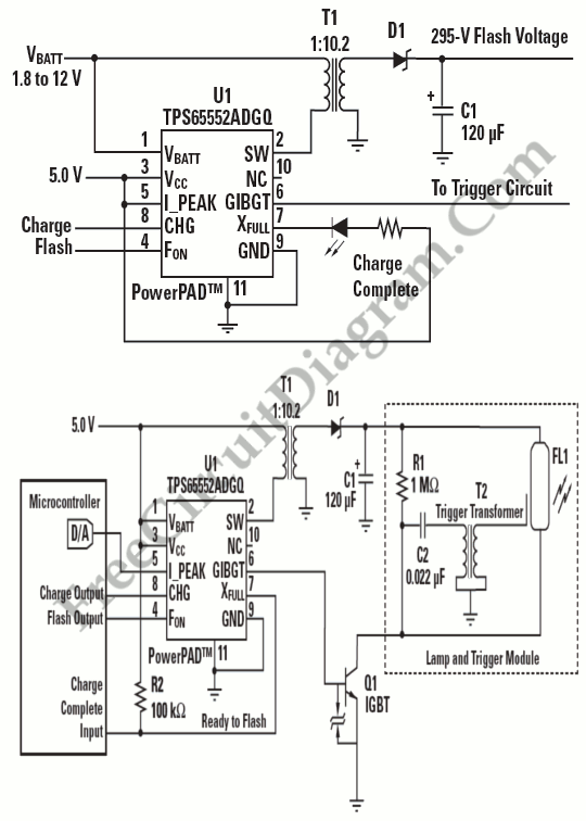
The size of the photoflash charger circuit is significantly simplified and reduced by the Texas Instrument (TI) TPS65552A. This device serves as a photoflash capacitor charger. The TPS65552A is a highly integrated photoflash capacitor charger designed to efficiently charge capacitors...
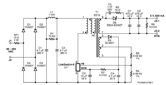
A simple 3.25W constant voltage/constant current (CV/CC) charger can be designed using the LinKSwitch family IC manufactured by Power Integrations. This electronic circuit project is intended to provide a 5-volt output with a maximum current of 650mA. The 3.25W...
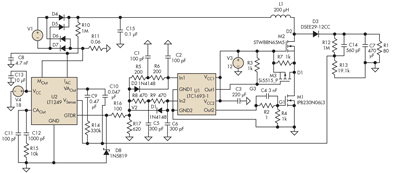
Adding a discharge path to the upper MOSFET of a cascode circuit significantly reduces the unavoidable Miller effect, thereby enhancing the Power Factor Correction (PFC) performance of a power supply's front end. In a cascode configuration, the upper MOSFET is...
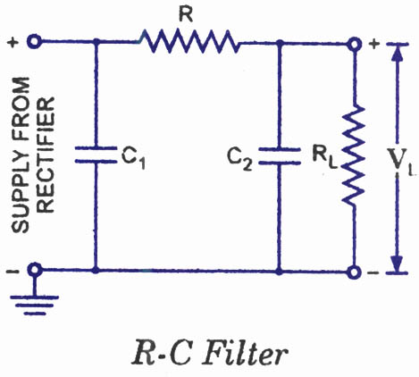
The disadvantages of pi-filters include higher costs, increased weight, larger size, and the external magnetic field generated by the series inductor. These issues can be mitigated by substituting the series inductor with a series resistor, referred to as an...
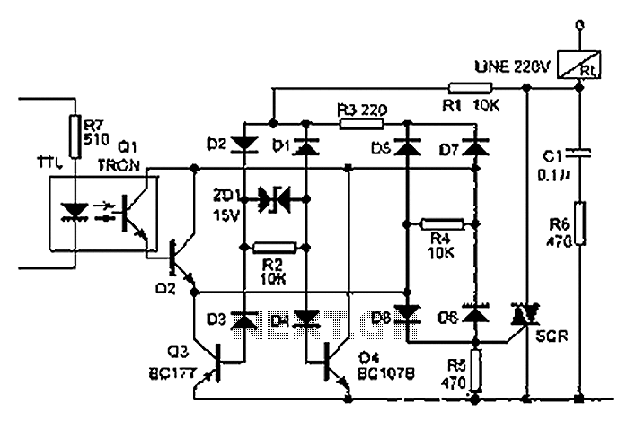
The relay illustrated in the figure operates based on non-inductive analog circuit theory. Its working principle involves a 220V power supply connected to a load (RL), resistors (R1, R3, R6), diodes (D1 to D8), and a zener diode (ZD1)....
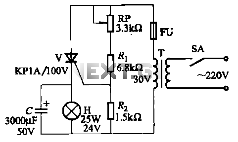
The circuit employs thyristor control. The flash frequency is determined by resistors Ri, RP, Rz, and capacitor C. By adjusting the electrical locator RP, the flash frequency can be varied from 0.5 Hz to several Hz. The described circuit utilizes...