
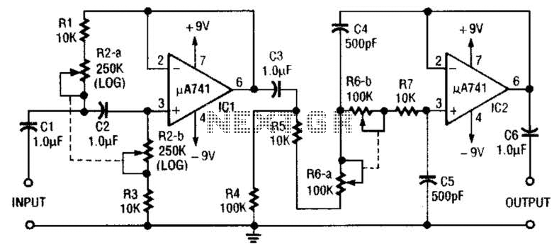
The Full-Wave Rectifier and Averaging Filter

The described circuit operates effectively as a precision AC voltmeter by utilizing a combination of rectification and amplification techniques. The full-wave rectification process is achieved through the arrangement of diodes and amplifiers, ensuring that both positive and negative input signals are accurately processed. The clamping action of diode D1 is crucial in maintaining the output voltage within a specified range, preventing distortion of the signal during negative cycles.
In the positive input scenario, the operation of amplifier A1 as a standard amplifier allows for the accurate amplification of the signal before it reaches the summing point of A2. The configuration of resistors R1 and R2 ensures that A2 functions as a unity gain inverter, effectively flipping the phase of the input signal while maintaining its magnitude. This is critical for accurately representing the RMS value of the AC input.
When examining the negative input path, the role of diode D2 becomes apparent as it isolates the output of A1 from A2, allowing the circuit to handle negative voltages without affecting the overall operation. The feedback loop involving resistors R3 and R5 is designed to maintain stability and accuracy, ensuring that the gain of A1 remains unaffected by variations in the input signal.
For applications requiring absolute value generation, the removal of capacitor C1 simplifies the circuit while still providing a reliable output. This modification is particularly useful in scenarios where only the magnitude of the AC voltage is of interest, eliminating the need to consider the sign of the input signal.
Overall, the careful selection of components and configuration of the circuit elements contribute to the reliability and accuracy of the AC voltmeter, making it suitable for various measurement applications in electronics.The heart of an average reading, rms calibrated AC voltmeter is shown in figure below. It`s a rectifier and averaging filter. We can remove the averaging function and provide a precision full-wave rectifier by deleting C2 and provide an absolute value generator by deleting C1. By following the signal path for negative and then for positive input, circuit operation may be understood. The output of amplifier A1 is clamped to +0. 7V by D1 and disconnected from the summing point of A2 by D2 for negative signals. A2 then will be behave as a simple unity gain inverter with input resistor, R1, and feedback resistor, R2. This will give positive going output. A1 operates as a normal amplifier connected to the A2 summing point through resistor R5 for positive inputs.
Then amplifier will behave as a simple unity gain inverter with input resistor R3 and feedback resistor R5. Since it is inside the feedback loop, A1 gain accuracy is not affected by D2. Negative current is drawn from A2 summing point through resistor R5 and positive current enters the A2 summing point through resistor R1.
The net input current at the A2 summing point is equal to and opposite from the current through R1 and amplifier A2 operates as a summing inverter with unity gain, again giving a positive input since the voltages across R1 and R5 are equal and opposite, and R5 is one half the value of R1. If the circuit is to used as an absolute value generator, capacitor C1 may be deleted. The circuit output will be the positive absolute value of the input voltage when this is done. For unity gain operation, the amplifiers chosen must be compensated. R6 and R7 must be selected to minimize output errors due to input offset current. [Source: National Semiconductor Application Note ] 🔗 External reference
Related Circuits
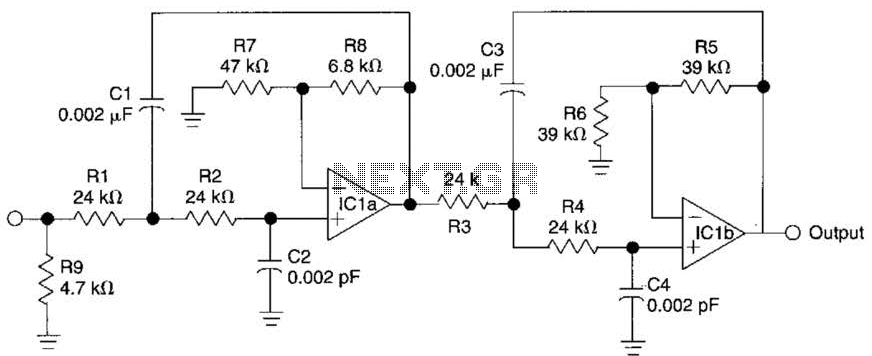
This circuit is a fourth-order low-pass filter designed for operation at kilohertz frequencies. The component values for resistors R1, R2, and capacitors C1, C2, as well as resistors R3, R4 and capacitors C3, C4 can be adjusted for functionality...
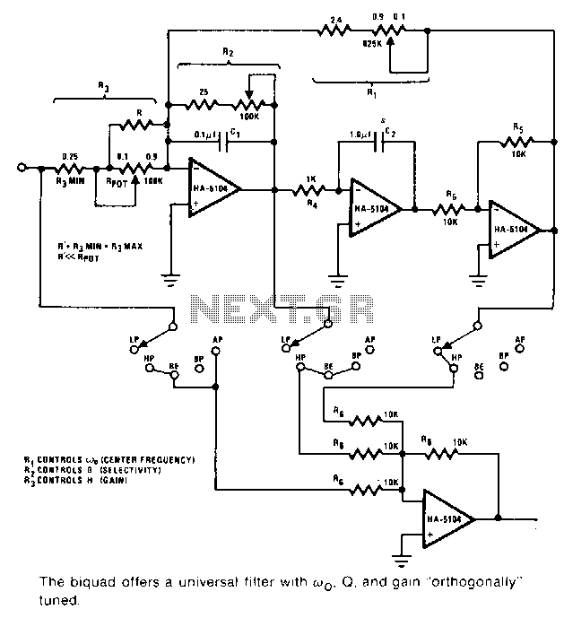
This universal filter provides low-pass, high-pass, bandpass, band elimination, and all-pass functions. The Biquad consists of two successive integration stages followed by an inverting stage. The entire system features a feedback loop from the front to the back, primarily...
These are operational amplifier (op-amp) based filters that are particularly effective within the audio frequency range. The calculators for these filters utilize formulas and tables from the book "Electronic Filter Design Handbook" by Arthur B. Williams. Bandpass filters allow...
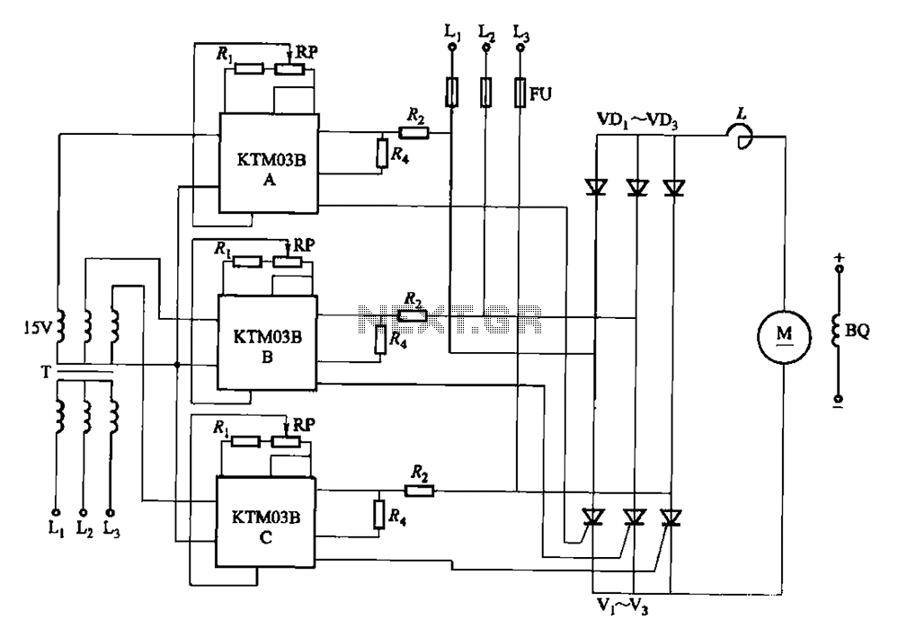
Adjusting the phase potentiometer RP can change the conduction angle of each corresponding thyristor (V1-V). This adjustment alters the voltage applied across the load. The circuit utilizes a phase control technique to manage the power delivered to a load by...
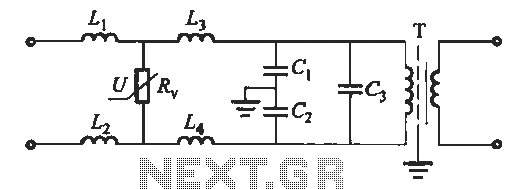
An isolation transformer is connected to a low-pass filter, with specific wiring configurations between them, as depicted in the accompanying figure. The low-pass filter is designed using inductors L1 to L4, which have values ranging from several to several...
This circuit is a variable audio bandpass filter that features a low cutoff adjustable from approximately 25 Hz to 700 Hz and a high cutoff adjustable from 2.5 kHz to over 20 kHz. The roll-off is set at 12...