
Touch delay switch a circuit diagram of a NAND gate consisting
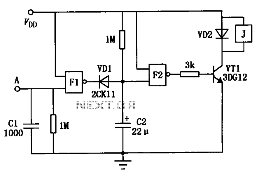
The touch delay switch circuit employs a CMOS NAND gate as its primary component, which is responsible for the logical operation and delay functionality. The circuit typically includes a capacitor, resistor, and a momentary switch to achieve the desired delay effect. When the switch is activated, the capacitor begins to charge through the resistor, creating a time delay before the output of the NAND gate transitions.
The configuration of the circuit ensures that the output remains low until the capacitor reaches a certain voltage level, at which point the NAND gate output will switch to high, activating the connected load, such as a light fixture. The time delay can be adjusted by changing the values of the resistor and capacitor, allowing for customization based on specific application requirements.
This design is particularly advantageous for applications in corridors and doorways, where automatic lighting can enhance safety and convenience. The use of CMOS technology ensures low power consumption, making the circuit efficient for prolonged use in residential and public lighting systems. As shown in FIG touch delay switch is a CMOS NAND gate composition, can delay about 10 seconds, often used in street corridor, home door lights automatic control.
Related Circuits
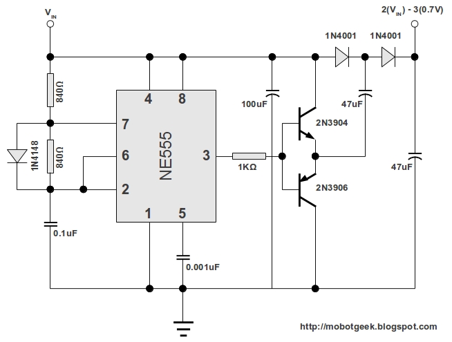
This DC voltage doubler circuit generates a voltage that is double its supply voltage. It is advantageous when a higher voltage level is required from a single lower voltage power supply. Due to the low current consumption in such...
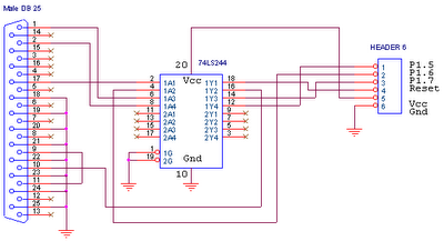
This circuit is designed for use with ATMEL Microcontroller ICs, specifically the AT89Sxx and ATMEGA series. It operates using the MISO, MOSI, SCK, and RESET signals. This circuit serves as a foundational interface for programming and communication with ATMEL microcontrollers,...
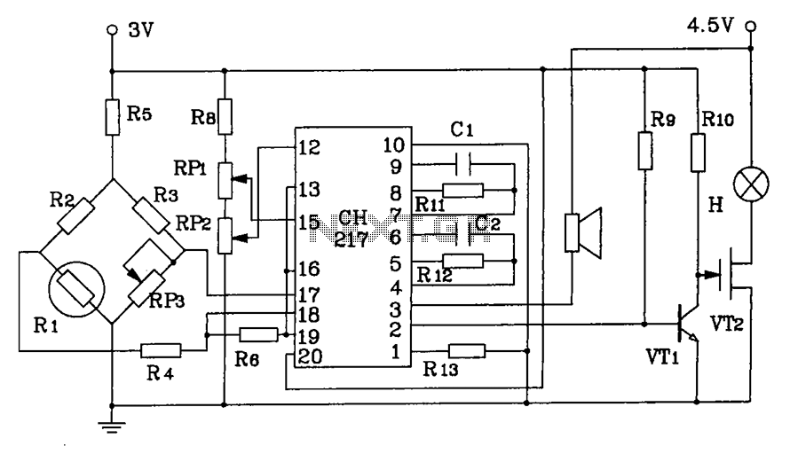
CH217 is a monolithic gas detection alarm integrated circuit. The gas detection alarm circuit diagram includes R1 as the gas sensing probe, where the resistance increases as the gas concentration decreases linearly. RP3 is used to adjust the output...
Design a circuit using a power MOSFET to replace the NTC thermistor that many Mag623 users employ to prevent their bulbs from flashing. Although inexpensive and easy to connect, NTCs run quite hot, are affected by ambient temperature, require...
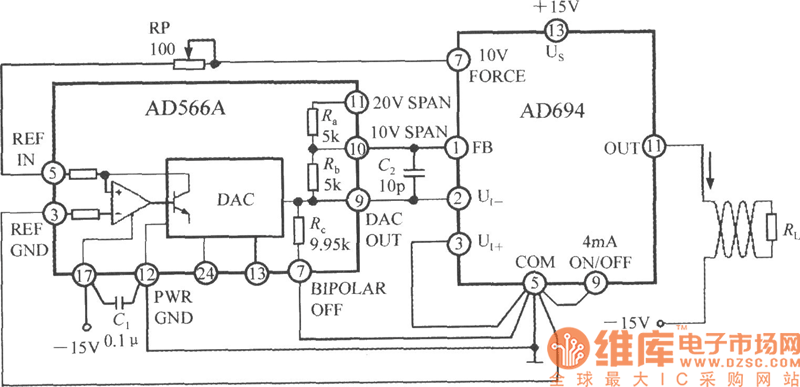
The current loop interface circuit diagram of the AD694 multi-functional sensor signal conditioner is utilized as a digital-to-analog converter (DAC). This current loop interface enables the conversion of digital values into voltage and subsequently into current signals. The circuit...
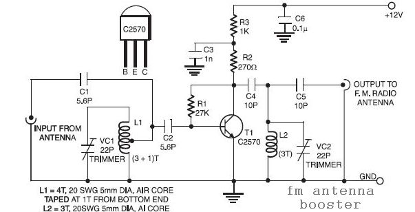
The input coil L1 is composed of four turns of 20 SWG enamelled copper wire, wound slightly spaced over a 5mm diameter former. It is tapped at the first turn from the ground lead side. Coil L2 is similar...
Warning: include(partials/cookie-banner.php): Failed to open stream: Permission denied in /var/www/html/nextgr/view-circuit.php on line 713
Warning: include(): Failed opening 'partials/cookie-banner.php' for inclusion (include_path='.:/usr/share/php') in /var/www/html/nextgr/view-circuit.php on line 713