
Touch light switch delay circuit
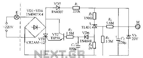
The touch-sensitive lamp delay circuit operates on the principle of capacitive coupling and thyristor triggering. The integration of the precision voltage regulator (T1.43 or AS431) ensures stable voltage levels, which are critical for consistent performance. When the circuit is idle, the thyristor VT1 remains in a non-conducting state, preventing any current flow to the lamp (E). The external switch terminal allows for easy integration into existing systems, making it a versatile solution for touch-activated lighting.
Upon touching the body (M), the resultant leakage current through resistor R initiates a sequence where the control electrode of the voltage regulator is activated. This leads to a rapid charging of capacitor C through the voltage regulator and diode (VD6), which is essential for providing the necessary trigger voltage to VT2. Once VT2 is activated, it allows current to flow through VT1, thus energizing the lamp (E).
The discharge path for capacitor C is designed to maintain the conduction state of VT2 even after the finger is removed. This is achieved through a carefully selected resistor (R) that controls the discharge rate, ensuring that the lamp remains lit until the stored charge diminishes below a critical level, at which point the thyristor VT1 will turn off as the AC current crosses zero.
The delay time, which is a critical parameter for user experience, can be adjusted by varying the values of resistors and capacitors in the circuit. The choice of components directly affects the sensitivity and responsiveness of the touch activation. For instance, using a thyristor with a low trigger current (such as the recommended Mitsubishi models) allows for a more responsive touch, while the selected transistors should be capable of handling the expected load without overheating.
In summary, this touch-sensitive lamp delay circuit is an efficient and innovative solution for modern lighting applications, combining minimal power consumption with user-friendly operation and customizable delay features.Is a good touch-down can delay the lamp, the circuit is characterized by: the static power consumption minimal; External switch terminal is only resistant to root, you can directly replace the ordinary switch, figure A novel precision voltage regulator integrated circuit T1.43 } or AS431, image only dressed leather outer seal pole tube, with the female usually the anode electrode between the non-conducting thyristor VT1 Ge broken pipe, lamp F does not shine. When a finger touches the body M when the leakage current flowing through R. , R. Partial pressure, was added to F1,431 control electrode so that T L131 quickly turned, 20V DC through R ,, TI.43l and VD6 to C.
Charging wells by R, muddy base VT2 eight poles, so that VT2 conduction, VT1 trigger current that is obtained while the opening of the lamp E on energized to emit light. After eight hand from M, Ct stored charge through R: v r2 to discharge, deceased mother maintain VT2 remain turned on, the lamp E will not be extinguished.
Until C- discharge current decreases, sufficient to maintain when conducting VT2, VT1 trigger the loss of current when the AC zero crossing, namely Ge broken lamp E goes out. Mainly by the delay time of the circuit G, R. Q. constant discharge decision. In addition, the trigger sensitivity of VT1 and VT2 magnification p value of Q has a great influence on the delay.
VT1 best Mitsubishi CR2AM-12 or CR3AS-12 micro-triggered thyristor way, as long as they have a touch shake 0_irnA current that can turn by the Secretary; VT2 should adopt Samsung TIP50 or MPSA-14 type _ = diode, requiring p / 50, when asked about the delay peel 70s around; the p 250, R. Selection of 4 7Mn H ten, uh delay time reaches 5m, n about.
Related Circuits
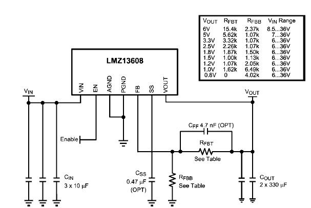
A simple, high-efficiency switching power supply circuit can be designed using the LMZ13608 8A regulator. This regulator offers very high efficiency and requires few external components. It supports a wide input voltage range of 6 to 36 volts and...
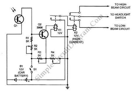
Automatic headlight dimmer circuit diagram for a car's headlight. This circuit ensures maximum brightness for optimal visibility while automatically switching when necessary. The automatic headlight dimmer circuit is designed to enhance driving safety by adjusting the brightness of the vehicle's...
The darkroom circuit is designed for one-time exposure and emits an audible signal when the developing time is reached. This circuit can be utilized for photofinishing large timers and other applications. It comprises components such as FET VTi, resistors,...
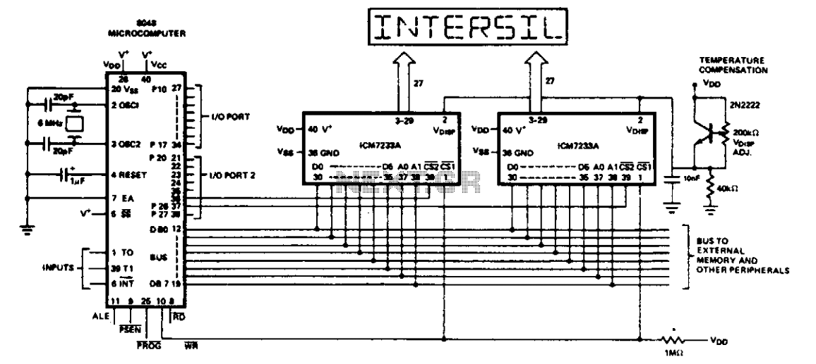
This is an 8048/IM80C48 microcomputer equipped with an 8-character, 16-segment ASCII triplex liquid crystal display. The two-bit character address is combined with the data and sent to the display driver under the control of the WR line. Port lines...
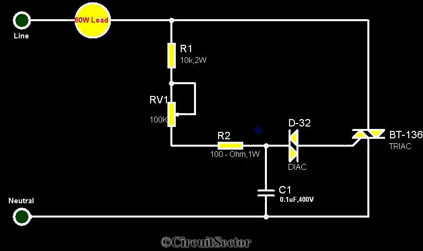
The circuit diagram presented is a triac-diac electronic fan regulator designed to reduce power consumption of electric fans, even at low speeds. Traditional resistor-inductor fan regulators tend to generate excess heat, wasting energy when the fan operates at lower...
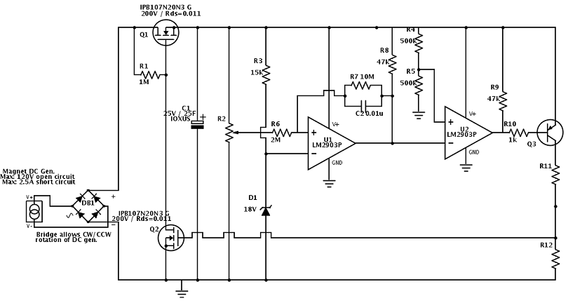
A flywheel-driven permanent magnet DC generator is used to charge a bank of supercapacitors rated at 35 farads and 25V. The maximum charge voltage is limited to 22V using a comparator and a zener reference due to the absence...
Warning: include(partials/cookie-banner.php): Failed to open stream: Permission denied in /var/www/html/nextgr/view-circuit.php on line 713
Warning: include(): Failed opening 'partials/cookie-banner.php' for inclusion (include_path='.:/usr/share/php') in /var/www/html/nextgr/view-circuit.php on line 713