
Solid State Switch for magnet DC Generator
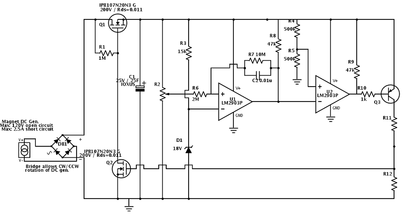
The circuit employs a flywheel-driven permanent magnet DC generator to efficiently charge a supercapacitor bank. The generator is capable of producing high voltage and current outputs, with safety mechanisms in place to limit the charge voltage to the supercapacitors. The use of a comparator and zener diode provides a reliable method to monitor and control the charging process, ensuring that the supercapacitors do not exceed their rated voltage.
The switching mechanism is critical to the operation of this circuit. The arrangement of Q1 and Q2 is designed to effectively manage the flow of current from the generator to the capacitor bank. The gate control of Q1 through a resistor allows for initial activation when the capacitor bank is at zero volts. As the voltage builds, Q3's activation leads to a change in Q2's state, which in turn influences Q1 to stop charging the capacitors, thus preventing overcharging.
Thermal management is an important consideration in this design, as the components can generate significant heat during operation. The introduction of a power resistor (Rs1) serves to limit the current and protect the circuit from excessive power draw. However, this also results in a trade-off, as it increases the time required to charge the capacitor bank. The addition of a diode (D3) is a precautionary measure to protect against potential reverse voltage conditions that could damage the power MOSFET.
Future enhancements to the circuit may include the implementation of a subcircuit to dynamically manage the load presented by Rs1, optimizing the charging efficiency while maintaining safe operating conditions for all components involved. This approach will ensure that the system operates reliably and efficiently, maximizing the performance of the flywheel-driven generator and the supercapacitor bank.Using a flywheel-driven permanent magnet DC generator to charge up a bank of supercapacitors, 35 farad rated to 25V. For safety I limit the max charge to 22V via a comparator and a zener reference. Because I have no stable reference voltage at all in in this system, I rely on the zener for a reference.
This small generator, at my max. RPM, put s out 120V open-circuit and 2. 5A short-circuit. Charging up from cap bank at zero volts, indeed 2. 5A flows into the cap bank and voltage climbs. When the voltage on the cap bank reaches 22V, comparator U1 goes high. U2 serves to invert this signal and turn on PNP Q3. I want to use the signal at Q3`s collector to drive some kind of switch to disconnect the charging current from the DC generator, in order to avoid over charging the cap bank. My question is on Q1 and Q2, my hypothetical switch. Does this approach make sense Starting from zero volts on the cap, I expect Q1 to be on as its gate is connected to is drain through the 1M resistor.
As soon as Q3 pulls up Q2`s Vg ~ 10V, I expect Q2 to pull down Q1`s Vg to near ground and effectively shut off charging current to C1. Due to feedback R7 & C2, U1 will not flip back again until ~ 20V. Let`s say that after charging C1 to 22V, Q1 goes into cutoff. Also, the DC generator is at a stop, so Vds = -22V Also, Vgs = -22V. I`m not sure if this condition will wreak havoc with Q1/Q2. The part number ( IP8107N20N3 G ) is spec`d for Vds = 200V and Vgs = +/- 30V but I`m not comfortable with that negative Vds on Q1.
Maybe I am going about this switching completely the wrong way. I`ve already burned out an SSR, which used to be in place of Q1, because my amateur experience forgot that when the load is removed from the generator, its open-circuit voltage climbs to 120V and my DC SSR was rated to switch only 60V. - When cap bank C1 is completely discharged, it presents a very large load to the DC permanent magnet generator.
Consequently, when Rs1 was not present, Vaa never climbed above ~8V at full RPM and thus Q1 never turns on fully; Q1 dissipates enough heat to get smoking hot in a few seconds w/o heatsink. I`m getting around this problem for the moment with a very large heat sink; the part will survive 175C but I really don`t want to get anywhere near that hot in the final design.
- Added Rs1, 3 ohm power resistor. With this load in place, Vaa climbs almost immediately to ~17V when generator is at speed. ( Generator is load-dependent & RPM dependent current and voltage source. ) So Q1 turns fully on. But the tradeoff is now Rs1 limits the available current to the cap bank. The charge time has increased for Vbb 0V->5V by about factor of 2. Not nice. - I needed to add D3 to counteract Q1`s built in body diode. I am only 95% sure I need D3, but I didn`t want to risk frying my power mosfet here. If the cap bank voltage Vbb is limited to 22V ( by U1 & U2, working OK ), and the generator is at standstill, that`ll give me -22V looking from Vbb to Vaa, effectively reverse biasing the power PFET. My next test will be to develop a subcircuit to short-out Rs1 once the cap bank reaches a charge level which will keep Vaa > 15V.
At this point I`m thinking another power NFET across Rs1`s terminals. 🔗 External reference
Related Circuits
This circuit can replace the single current-limiting resistor commonly found in inexpensive battery chargers. The alternative presented here will prove beneficial as it prevents the premature disposal of NiCd batteries after approximately three months of inadequate charging. The circuit...
V1 and V2 are set to 5V in the simulation, but they could also be set to 10V to eliminate the need for a second power supply. Alternatively, if logic level FETs can be sourced at that higher voltage,...
A circuit was assembled on a breadboard, which is divided into two sections. The right section is dedicated to generating a wailing alarm, while the left section is... The circuit design comprises two main functional blocks: the alarm generation circuit...
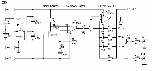
White noise (the sound you hear when a TV is tuned to a non-existent station) has a frequency characteristic which raises the power level by 3dB with each increasing octave, and is not suitable for response testing (and will...
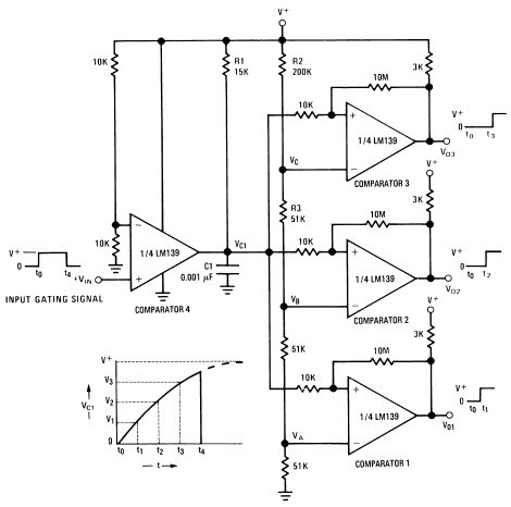
A measure delay generator, also identified similarly to a sequence generator, is a device that provides output signals at specified time intervals from a time reference. It automatically resets when the input signal returns to ground. The schematic illustrates...

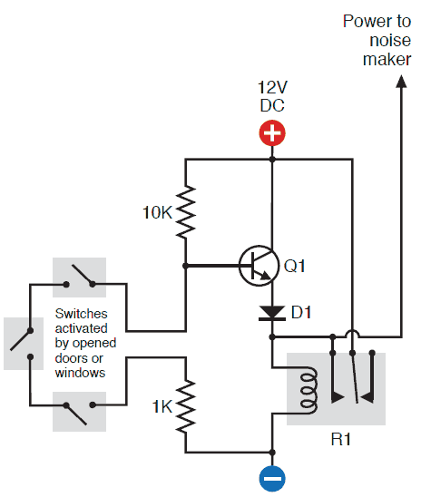
In the example above, a low voltage (12V DC) is utilized to activate a relay that switches a 240V AC main circuit. It is important to note that there is no electrical connection between the two circuits within the...