
Transformerless 5 Volt Power Supply circuit
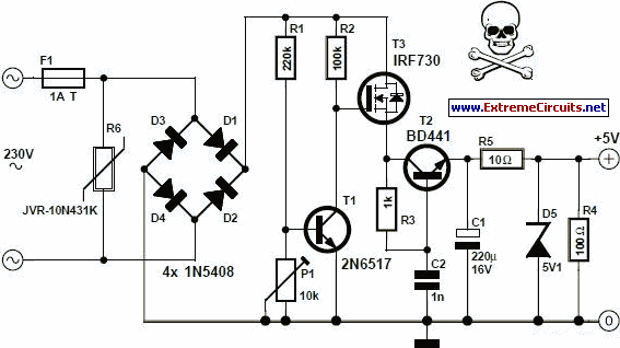
The circuit design described facilitates a compact and efficient solution for powering low-consumption devices directly from the mains supply. The use of a JVR varistor ensures overvoltage protection, safeguarding the circuit from surges that could damage sensitive components. The voltage divider formed by resistors R1 and R2 is critical in determining when the main switching transistor (T1) activates, allowing for precise control over the output voltage and current characteristics. The interaction of T1 and T3 is essential for managing the flow of current to the reservoir capacitor (C1), which smooths out the rectified voltage and provides a stable output.
The soft start mechanism, implemented through T2, R3, and C2, is particularly important for applications where sudden inrush currents could lead to component failure or circuit instability. This feature allows the power supply to ramp up gradually, minimizing stress on the components during power-up. The zener diode (D5) not only regulates the output voltage but also acts as a protective measure for the capacitor, ensuring that it operates within safe voltage limits.
The design's reliance on a minimal number of components while achieving its goals of efficiency and reliability makes it an attractive option for low-power applications. However, the inherent risks associated with working directly with mains voltage necessitate careful consideration and adherence to safety protocols. The circuit's simplicity and effectiveness illustrate a practical approach to power supply design for modern low-power devices, balancing performance with component protection.An increasing number of appliances draw a very small current from the power supply. If you need to design a mains powered device, you could generally choose between a linear and a switch-mode power supply. However, what if the appliance`s total power consumption is very small Transformer-based power supplies are bulky, while the switchers are gen
erally made to provide greater current output, with a significant increase in complexity, problems involving PCB layout and, inherently, reduced reliability. Is it possible to create a simple, minimum part-count mains (230 VAC primary) power supply, without transformers or coils, capable of delivering about 100 mA at, say, 5 V A general approach could be to employ a highly inefficient stabilizer that would rectify AC and, utilizing a zener diode to provide a 5.
1 V output, dissipate all the excess from 5. 1 V to (230G—v2) volts in a resistor. Even if the load would require only about 10 mA, the loss would be approximately 3 watts, so a significant heat dissipation would occur even for such a small power consumption. At 100 mA, the useless dissipation would go over 30 W, making this scheme completely unacceptable. Power conversion efficiency is not a major consideration here; instead, the basic problem is how to reduce heavy dissipation and protect the components from burning out.
The circuit shown here is one of the simplest ways to achieve the above goals in practice. A JVR varistor is used for overvoltage/surge protection. Voltage divider R1-R2 follows the rectified 230 V and, when it is high enough, T1 turns on and T3 cannot conduct. When the rectified voltage drops, T1 turns off and T3 starts to conduct current into the reservoir capacitor C1.
The interception point (the moment when T1 turns off) is set by P1 (usually set to about 3k3), which controls the total output current capacity of the power supply: reducing P1 makes T1 react later, stopping T3 later, so more current is supplied, but with increased heat dissipation. Components T2, R3 and C2 form a typical soft start` circuit to reduce current spikes this is necessary in order to limit C1`s charging current when the power supply is initially turned on.
At a given setting of P1, the output current through R5 is constant. Thus, load R4 takes as much current as it requires, while the rest goes through a zener diode, D5. Knowing the maximum current drawn by the load allows adjusting P1 to such a value as to provide a total current through R5 just 5 to 6 mA over the maximum required by the load. In this way, unnecessary dissipation is much reduced, with zener stabilization function preserved. Zener diode D5 also protects C1 from over voltages, thus enabling te use of low-cost 16 V electrolytics.
The current flow through R5 and D5, even when the load is disconnected, prevents T3`s gate-source voltage from rising too much and causing damage to device. In addition, T1 need not be a high-voltage transistor, but its current gain should exceed 120 (e. g. BC546B, or even BC547C can be used). The circuit is not galvanically isolated from the mains. Touching any part of the circuit (or any circuitry it supplies power to) while in operation, is dangerous and can result in an electric shock!
This circuit should not be built or used by individuals without proper knowledge of mains voltage procedures. 🔗 External reference
Related Circuits
The Chizuru 100Hz channel frequency pulse charging circuit for electric bike batteries is designed to manage the charging process efficiently. It features a step-down transformer (Tl) and a bridge rectifier formed by diodes D5 to D8. The output ripple...

This design circuit is a tachometer circuit based on the LM2907 integrated circuit, which can provide zero-crossing data to a digital system. At each zero crossing of the input signal, the charge pump alters the state of capacitor C1...
Nokia BL-4C and BL-5C are 3.7V, 700-1000mAh (various) lithium-ion batteries that have three terminals. These terminals include a positive terminal, a ground, and a BSI (Battery Status Indicator) terminal, which presents a fixed resistance value that needs to be...
This electret microphone amplifier is constructed using standard electronic components. It is designed to work with an electret microphone capsule, although it can also accommodate a dynamic microphone that has low resistance. The circuit operates with a supply voltage...

The AD524 is a low-drift instrumentation amplifier characterized by a drift voltage of 0.5 mV and a maximum drift of 25 mV at room temperature. It has low noise performance with a noise level of 0.3 mVp-p in the...

A neon lamp can easily be added to the phone line to act as a ring indicator. It is perfect for times when you cannot hear the phone. The integration of a neon lamp as a ring indicator in a...