
TV as display terminal interface circuit diagram

The described interface circuit serves as a vital link between a computer's video output and a television display, ensuring compatibility and enhancing signal strength. The circuit's primary function is to amplify the standard video signal from 1V (Peak-to-Peak) to a more robust 3V (Peak-to-Peak), which is often necessary for optimal display performance on larger screens or for longer cable runs.
The negative feedback mechanism, implemented through transistors T1 and T2, plays a crucial role in stabilizing the gain and maintaining linearity across a broad frequency range. This design choice minimizes distortion and ensures that the amplified video signal retains its original quality, which is essential for applications requiring high fidelity, such as video presentations or gaming.
The amplification factor, or gain, of the circuit is adjustable based on the resistor values R1 and R2. By manipulating these resistors, the designer can fine-tune the circuit's response to meet specific requirements. The choice of R1 and R2 directly influences the time constant of the circuit, impacting how quickly the circuit can respond to changes in the input signal, thereby affecting the overall performance and responsiveness of the video output.
Overall, this interface circuit is an effective solution for enhancing video signal strength while preserving quality, making it an essential component in various electronic systems that require reliable video output.The interface circuit is added between computer standard video signal output terminal and TV. It can enlarge standard 1V(Peak - peak) video signal am to 3V(Peak - peak). Negative feedback circuit is composed of T1 and T2. It has a wide frequency range. The enlarge time is decided by the ratio of R1 and R2.. 🔗 External reference
Related Circuits
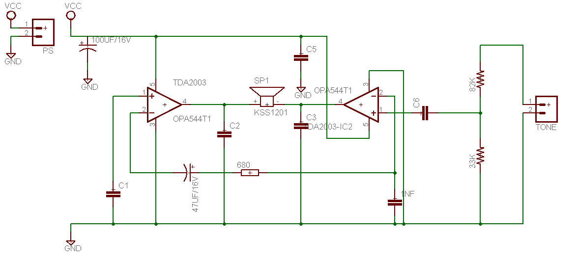
This is a design for a tone control circuit. The circuit features the LM1036, which is a DC-controlled tone (bass/treble), volume, and balance circuit suitable for stereo applications in car radios, televisions, and audio systems. The LM1036 integrated circuit is...
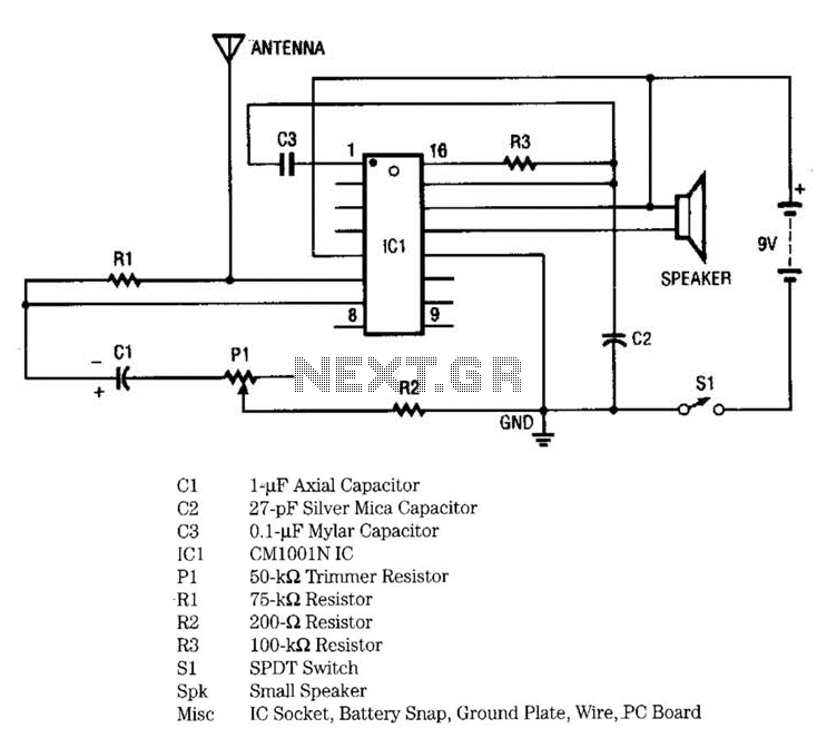
IC1 includes multiple oscillators and an amplifier. The low-frequency audio signal oscillator provides an input to the amplifier. This signal is the audio tone that is amplified and subsequently delivered to the speaker by the amplifier. The high-frequency oscillator...
When the power supply reaches the circuit and the input signal is applied, the sound signal is processed through capacitor C1 and resistor R1 for signal coupling and noise reduction. The modified signal then reaches pin 3 (non-inverting) of...
It is essential to draw a circuit using a layout and conventions that are universally recognized. In electronic circuit design, adherence to standardized symbols and layout conventions is crucial for effective communication among engineers and technicians. A well-drawn schematic diagram...
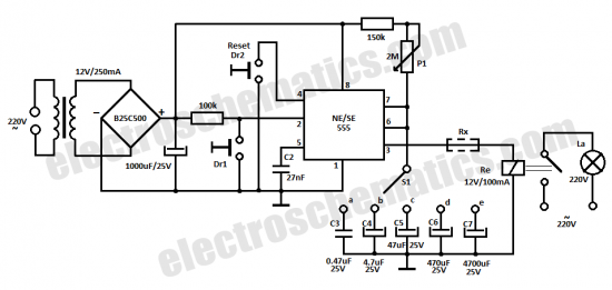
This time delay relay circuit is constructed using the NE/SE555 integrated circuit, manufactured by Intersil, which incorporates a precision timer. The circuit exhibits stability against temperature variations of 0.00. The NE/SE555 timer IC is a versatile device widely used in...
Building circuits to interface an Amiga A1200 to a PC AT/ATX power supply and tower case. To create a reliable interface between an Amiga A1200 and a PC AT/ATX power supply and tower case, it is essential to design a...