
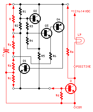
Two-phase squarewave oscillator
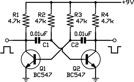
The astable multivibrator circuit is composed of two NPN transistors (Q1 and Q2), resistors (R1, R2, R3, and R4), and capacitors (C1 and C2). The transistors are configured in a feedback loop that allows for continuous oscillation. The resistors serve to limit current and set the charge and discharge rates of the capacitors, while the capacitors determine the timing intervals of the oscillation.
To construct the circuit, connect the emitters of both transistors to ground. The collector of Q1 connects to the junction of R1 and C1, while the collector of Q2 connects to the junction of R3 and C2. The base of Q1 is connected to the junction of R2 and C1, and the base of Q2 is connected to the junction of R2 and C2. The resistors R2 and R3 are connected to a positive voltage supply, typically 9V.
The oscillation frequency can be adjusted by varying the values of the resistors and capacitors. The relationship between the timing components can be expressed using the formula for frequency:
\[ f = \frac{1.44}{(R1 + 2R2) \cdot C1} \]
This equation illustrates how the frequency of oscillation is inversely proportional to the total resistance and capacitance in the circuit. The output can be taken from the collectors of both transistors, providing two square wave signals that are 180 degrees out of phase with each other. This characteristic makes the astable multivibrator suitable for applications such as clock pulses, tone generation, and signal modulation.
In summary, the astable multivibrator circuit is a fundamental electronic oscillator that demonstrates the principles of transistor switching and capacitor charging and discharging. Its simplicity and versatility make it a valuable tool in various electronic applications.It`s one of the simplest circuits to get working but one of the more tricky to understand. This simple two-transistor oscillator has a technical name of astable multivibrator and provides a squarewave (of sorts) output in and out of phase. First up, keep in your mind that capacitors cannot change their voltage instantly. So we`ll assume that th e cap attached to R2 has 0V across it. This pulls the base of Q2 to 0V, which means it`s off. However, with Q1 on, that 0. 01uF capacitor now begins to charge via R2. When the voltage at the junction of the cap and R2 (which is also the base of Q2) reaches 0. 6V. This now turns Q2 on. Because Q1 was on, that means the cap joining R3 had 0. 6V across it (it can`t go any higher because the Vbe drop of Q1 won`t let it go higher than 0. 6V) but Q2 switching on effectively pulls the side of the capacitor connected to R4 from 9V down to 0V. As I said before, capacitors cannot instantly change the voltage across them so what happens on the R3 side of capacitor C2 is its voltage goes from 0.
6V down to -8. 4V, which well and truly turns Q1 off. At the same time, a similar thing has happened to cap C1, connected to R1 and R2. The R1 side of that cap has jumped from 0V to 5VDC and the other side jumps from 0. 6V to 5. 6V well, it would if it wasn`t for the Vbe junction of Q2, which holds it to 0. 6V. So now that Q2 is on and Q1 is off, C2 now begins charging up via R3 and the Q2 collector-emitter path. But it`s starting from -8. 4V and it has to reach 0. 6V before it turns Q1 back on again. However, it will eventually do so, turning Q1 on, which pulls the R1 side of C1 from 9V down to 0V and the R2 side from 0.
6V to -8. 4V. How the circuit actually starts in practice is going to be a bit of a lottery, even with component pairs the same as shown above. What actually happens in practice is that as soon as the power is applied, there`s a race between the two RC combinations (R2/C1 and R3/C2) to see whichever one reaches 0.
6V first. The one that does turns on the opposite transistor first (eg R2/C1 turns on transistor Q2 or R3/C2 turns on Q1), which forces the other transistor off. And as soon as we reach that state, the circuit gets into a groove and off it goes. Because the transistors operate in opposite states (eg. Q1 is off when Q2 is on and vice versa), you actually get dual outputs from the two collectors that are out of phase.
This can be very handy in plenty of circuits. Of course, you could also connect a speaker to the emitter of Q1 (make it a BC337) and provided you choose the right R/C values, you`ll hear a tone coming from it. And if you wanted to be able to electronically control turn this on and off, lift up the +V rail ends of resistors R2 and R3 and drive them with the output of some other circuit.
When the tops of those resistors are pulled to ground, the circuit stops but pull them up to the positive rail as shown, and it operates as normal. This is actually one of three similar circuits of the multivibrator family. Later, we`ll look at the monostable multivibrator that produces a pulse for a set period when triggered.
🔗 External reference
Related Circuits
Signals with a known frequency but an unknown phase can be detected using an in-phase signal and a signal that is shifted by 90 degrees, a method commonly utilized in lock-in amplifiers, synchronous detectors, and frequency-response analyzers. The signal...
Many RC oscillators utilize advanced circuits within the phase shift unit. These circuits employ voltage feedback amplifiers, whose gain decreases significantly at high frequencies and ceases when high frequency is not attained. The variation in the phase characteristics of...
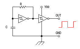
The hysteresis characteristic indicates that the voltage level transitions to high (H) when the input voltage of the inverter rises from 0 V, and the voltage level transitions to low (L) when the input voltage descends from +5 V....
The 8-lead plastic mini-DIP LM3909 integrated circuit was developed by National Semiconductor in the mid-1970s. It is a monolithic oscillator specifically designed to flash Light Emitting Diodes (LEDs). By utilizing the timing capacitor for voltage boosting, it can deliver...

This circuit generates sine and square wave signals with frequencies ranging from below 20 Hz to above 20 kHz. The advantage of this circuit diagram is that the output frequency can be adjusted by varying the variable resistor R6. The...
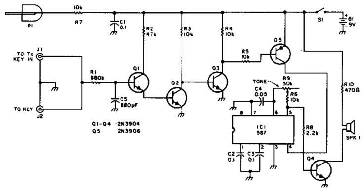
For use with low-power transmitters that require a positive keying voltage. The transistors Q1, Q2, and Q3 are configured as a switching amplifier. When the key is pressed, the collector of Q3 is pulled to ground, which activates Q5...