
Square wave oscillator
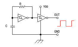
The hysteresis behavior in an inverter circuit is critical for ensuring stable operation and preventing oscillations due to noise in the input signal. In this context, the inverter has two distinct threshold voltages: the upper threshold voltage (Vth+) and the lower threshold voltage (Vth-). When the input voltage rises from 0 V, the output switches from low to high at the upper threshold voltage. Conversely, as the input voltage decreases from +5 V, the output transitions back from high to low at the lower threshold voltage.
This difference between Vth+ and Vth- creates a region of stability that helps to mitigate the effects of noise and provides a clear demarcation between the high and low states. The hysteresis effect can be enhanced by incorporating feedback into the inverter design, which can be achieved using resistors or additional components such as Schmitt triggers.
For practical applications, the specific values of Vth+ and Vth- can be adjusted by selecting appropriate resistor values in the feedback loop or by using specific components designed to provide desired hysteresis characteristics. This can be particularly useful in digital circuits where signal integrity is paramount, as it ensures that the output remains stable despite minor fluctuations in the input signal.
Overall, understanding and implementing hysteresis in inverter circuits is essential for achieving reliable performance in various electronic applications, such as signal conditioning, waveform shaping, and noise immunity in digital systems.By the hysteresis characteristic, the voltage which becomes the H level with the input voltage of the inverter rising from 0 V (Voltage that the output becomes 0 V) and the voltage which becomes the L level, descending from +5 V (Voltage that the output becomes +5 V) are different. 🔗 External reference
Related Circuits

C1 takes the DC-decoupled voltage from the microphone, amplifies it via Q1, then C2 decouples it again. R6 and C3 form a low-pass filter, but once the signal reaches Q2, the circuit accomplishes frequency modulation. The frequency deviation is...
This circuit is a 1024 kHz temperature-compensated crystal oscillator. The circuit theory is illustrated. Due to the low output signal level of the circuit, a buffer using the following transistor VT1 is implemented for amplification. The base bias resistor...
This circuit can be utilized as a light detector and potentially as a tool for individuals with visual impairments. The frequency of the oscillator is influenced by the level of illumination received by LDR4. The circuit operates by employing a...
This oscillator employs two transistors and operates the crystal in its fundamental mode. Capacitors CT and C2 should be approximately 2,700 pF for 1 MHz, 680 pF for 5 MHz, and 330 pF for 10 MHz. A capacitance of...

An early schematic of a Colpitts circuit utilizing a vacuum tube, redrawn from a patent publication. The Colpitts oscillator, invented in 1920 by American engineer Edwin H. Colpitts, is one of several designs for electronic oscillators. The Colpitts oscillator is...
In previous discussions, simulations of half-wave and full-wave rectifiers using standard diodes were presented. This post transitions to the power electronics domain, focusing on a Single Phase Half-Wave Rectifier utilizing a thyristor, also known as a Silicon Controlled Rectifier...