
Unity gain Inverter amplifier circuit

Additionally, the resistances in the range of 4.7 to 220 ohms at the LT1022 serve as a voltage divider to prevent excessive input overdrive during startup. This circuit integrates the LT1012, which has a noise level of 35 pV and an offset drift of 1.5 to 23 µV/°C, with the LT1022, which features a slew rate of 300 V/µs and a bandwidth of 300 kHz for full power operation. The bias current, primarily influenced by the LT1012, is approximately 100 pA.
The described circuit is a precision analog signal processing system that leverages the characteristics of both the LT1012 and LT1022 components. The LT1012, known for its low offset voltage and low drift, is ideal for applications requiring high accuracy and stability in low-frequency environments. The integration of a capacitor at the LT1012's output allows for the filtering of high-frequency noise, ensuring that only the desired low-frequency signals are processed.
In contrast, the LT1022 amplifier is optimized for high-speed applications, capable of handling rapid changes in input signals with minimal distortion. The feedback mechanism established through the summing node allows for real-time adjustments, ensuring that the output remains stable even with variations in input conditions. The use of a resistor divider at the LT1022 input is a critical design choice, as it mitigates the risk of overdriving the amplifier during power-up, thus protecting the circuit from potential damage.
Overall, this circuit design exemplifies the careful consideration of component characteristics and operational parameters, resulting in a robust solution for applications requiring both low-frequency stability and high-frequency responsiveness.The circuit consists of a device with low drift LTl012. and a speed amplifier LTl022Jligh. The entire circuit is a unity gain inverter, with the summing node at the junction of three resistors 10k. The monitors what the Tl012 summing node, it compares to the mass, and drives the positive input LTI022, completing a loop to stabilize around the Tl022 L.
The k 10 to 300 pF at the time constant LTI012 limit its response to low frequency signals. LTl022 handles the high-frequency inputs while LTl012 stabilizes the operating point. The k from 4.7 to 220 ohms at Tl022 The divider prevents excessive input overdrive at startup. This circuit combines LTl012 of 35 pV and offset drift of 1.5 to 23 REFER LTl022 V / ps slew rate and 300 kHz bandwidth for full power. bias current, dominated by the LTl012, is about 100 pA.
Related Circuits
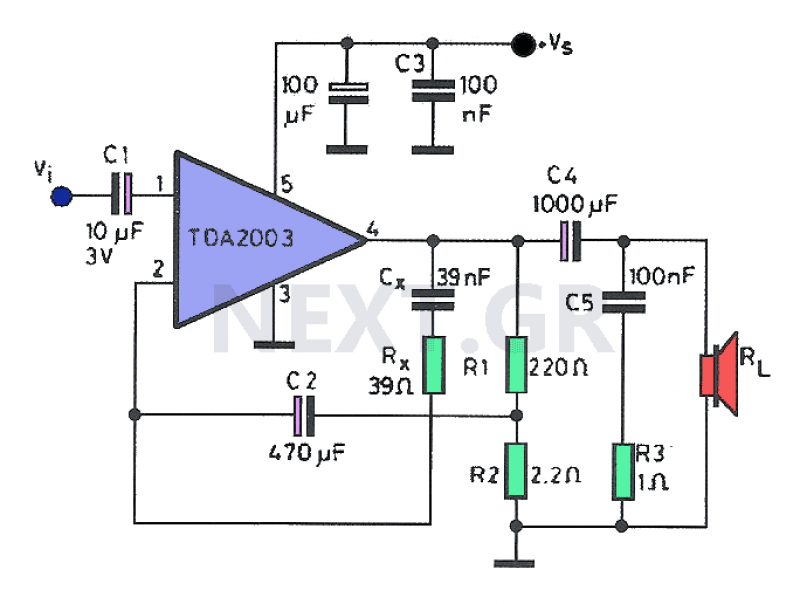
Often, a small amplifier is required to accommodate the needs of compact spaces. This amplifier can be configured as either mono or stereo, and its circuitry is capable of efficiently driving two small speakers. Constructing the amplifier necessitates only...
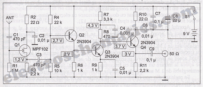
This is a wideband shortwave (SW) antenna amplifier. The frequency range spans from 1 to 30 MHz, featuring a medium gain of 15 dB. The input stage utilizes an MPF102 transistor. The wideband shortwave antenna amplifier is designed to enhance...
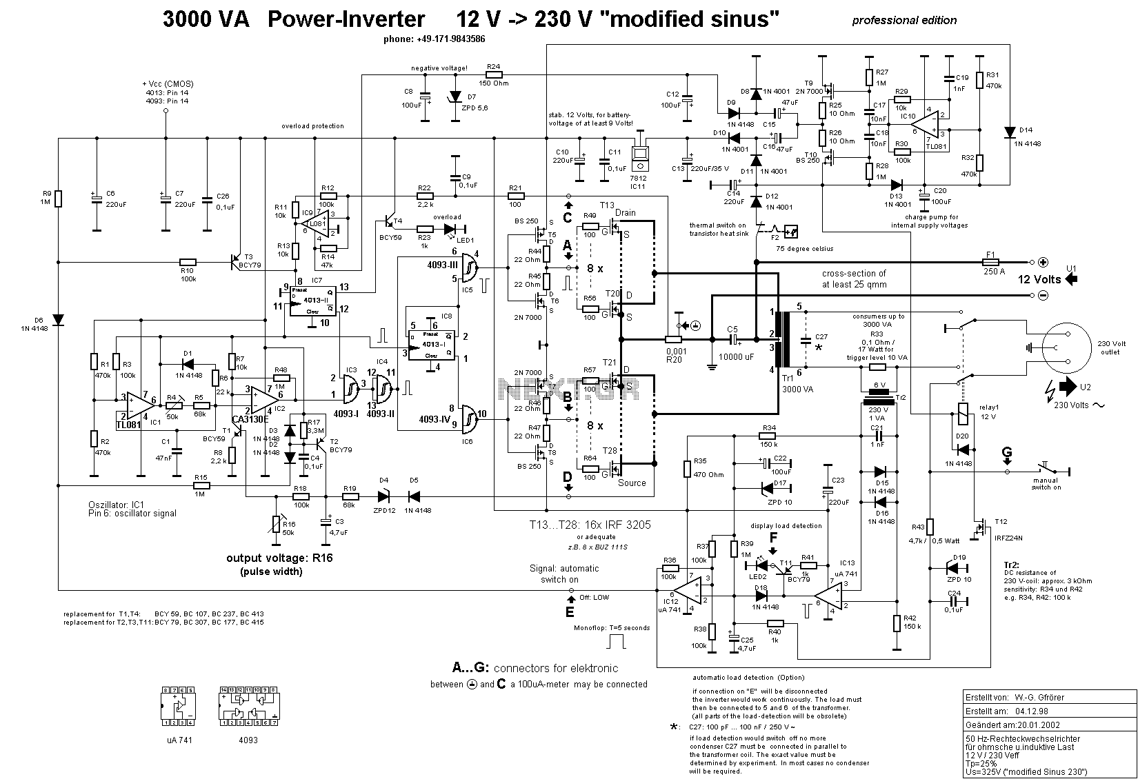
This is a high-power inverter circuit designed to deliver an AC power output of 3000W. It converts 12 Volt DC battery voltage into a square wave voltage with a frequency of 50 Hz and a duty cycle of 25%. The...
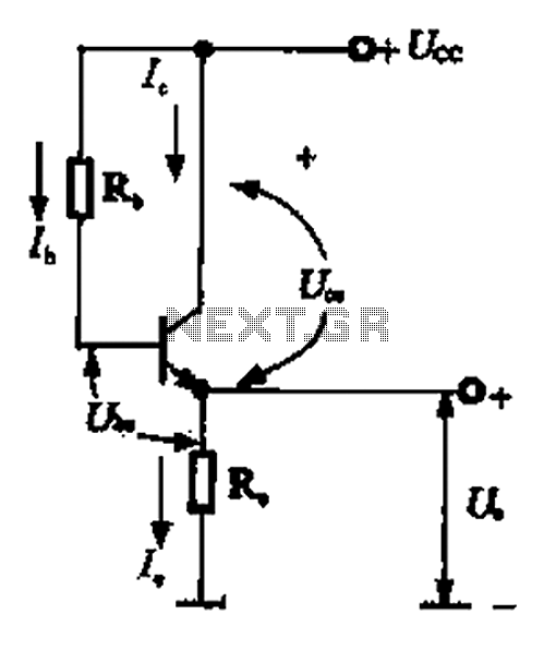
A common collector amplifier can be analyzed through its DC and AC paths, as illustrated in Figure 1-14. The DC path is responsible for providing a biasing circuit for the power transistor, determining whether the transistor is in an...
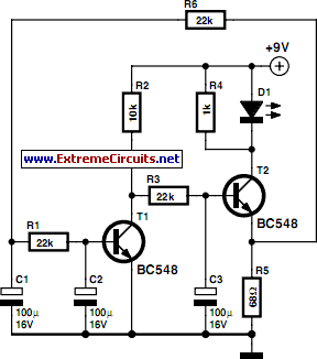
Standard LED flashers activate the LED in a rapid on-off sequence, which can become bothersome over time. The circuit presented here offers a more gradual illumination effect. This circuit utilizes a simple design to create a soft flashing LED effect,...
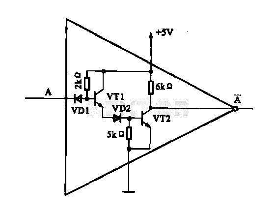
The internal structure of the DTL inverter circuit (M5936P) is composed of inputs with diodes and transistors for signal processing, powered by a +5V supply. When the input terminal A is at a high level (digital 1), diode VDI...