
Using AD9835 DDS chip with BASIC-52

The AD9835 chip is a versatile component capable of generating precise sine wave outputs suitable for a variety of applications, including RF signal generation and audio synthesis. The internal architecture consists of a phase accumulator that allows for the generation of different frequencies by adjusting the input values. The sine wave table provides the necessary data for outputting the desired waveform, while the 10-bit DAC converts the digital signal to an analog output.
To implement the AD9835 in a circuit, it is essential to adhere to the recommended power supply configurations and grounding practices to minimize noise and interference. The separation of analog and digital grounds is crucial in maintaining signal integrity, particularly in high-frequency applications. Filtering the AVDD power supply with appropriate capacitors will further ensure stable operation.
The integration of the AD9835 with an 8052 microcontroller allows for flexible control over the output frequency and phase. The provided code snippets demonstrate how to initialize the chip, set the desired output frequency, and transmit command words to the AD9835. The use of subroutines simplifies the process of calculating the frequency register values and programming the frequency registers, making it accessible for both novice and experienced users.
In summary, the AD9835 is a powerful DDS chip that can be effectively utilized in various electronic applications. Proper attention to circuit design, component selection, and programming will enable users to harness the full potential of this device for generating high-quality sine wave signals.AD9835 is a DDS (direct digital synthesis) chip from Analog Devices. It contains a phase accumulator, sinewave table, and 10-bit D/A converter. In can be used for phase and frequency modulation by selecting the phase and frequency of the signal either under software control, or using I/O pins (4 phases, 2 frequencies). Although the chip is designe d for RF applications, it makes a good audio frequency sinewave generator, too. The schematics below shows how to hook it up to 8052-BASIC chip. The circuit is quite straightforward. MCU clock is used as master clock for DDS, control interface is connected to PWM_OUT, T2EX, and T2. Phase and frequency selector pins are not used in this application, so they are tied to ground. Resistor and capacitor values are straight out of a datasheet schematics. Do filter the AVDD power supply, and keep the analog and digital grounds separated, connect them in single point as close to power supply as possible. The output voltage that is developed on R1 is between ground and REFIN (about 1. 2V with internal reference used by connecting REFOUT to REFIN). AD9835 comes in TTSOP-16 package (0. 65mm pin spacing), and only that. You probably need some magnifying equipment to work with it (depending on your eyesight and steadiness of your hand).
I just scanned the result with flatbed scanner at 1200dpi and examined the result. In general, the best option for prototyping in my opinion is a `format conversion`. This is how I usually do it. I soldered the DIP-24 socket on veroboard, then cut a suitable size piece of a board and placed it over the socket. I then stuck a wire into socket through the board, soldered and trimmed the wire. The end result is a crude DIP-24 package. I then scraped the pads off from where the TTSOP case needed to go, and soldered wires to `dip24` terminals from each of the pins.
Finally I soldered power supply decoupling caps directly to the converter board. AD9835 has a built-in `suicide switch` which activates when you short the output to VDD or AVDD. All the magic smoke comes instantly out of a chip, and you have to start all over. Not to mention a loss of your hard-to-get chip. 10 REM AD9835 control v1 15 REM reset chip 16 PRINT "Initializing. " 20 CW=0F800H : GOSUB 1000 30 CW=0B000H : GOSUB 1000 32 CW=05000H : GOSUB 1000 33 CW=04000H : GOSUB 1000 35 REM clear phase reg 0 40 CW=01800H : GOSUB 1000 50 CW=00900H : GOSUB 1000 55 REM set default frequency to 1000 Hz 60 F=1000 : GOSUB 2000 : GOSUB 3000 95 REM enable chip 100 CW=0C000H : GOSUB 1000 190 REM main loop 200 PRINT "Output frequency set to ", INT(FW)*CX, "Hz" 210 INPUT "Enter desired frequency (Hz) ", F 220 GOSUB 2000 : GOSUB 3000 230 GOTO 200 999 END 1000 REM send CW to AD9835 1010 PORT1=0BFH : PORT1=0BBH : FOR I=1 TO 16 1013 BT=0 : IF CW>32767 THEN BT=1 1016 CW=CW. AND. 7FFFH : CW=CW+CW 1020 PORT1=0BAH. OR. BT : PORT1=0B8H. OR. BT : PORT1=0BAH. OR. BT 1040 NEXT I : PORT1=0BFH 1060 RETURN 2000 REM calculate DDS freq register values to FH, FL 2001 REM desired frequency is in F 2020 CX=XTAL/(2*32) 2030 FW=F/CX 2035 FW=FW+0.
5 2040 FH=INT(FW/65536) 2050 FL=INT(FW-(FH*65536) 2070 RETURN 3000 REM program FREQ0 using FH, FL 3010 CW=FL. AND. 255 : CW=CW. OR. 03000H : GOSUB 1000 3020 CW=INT(FL/256) : CW=CW. OR. 02100H : GOSUB 1000 3030 CW=FH. AND. 255 : CW=CW. OR. 03200H : GOSUB 1000 3040 CW=INT(FH/256) : CW=CW. OR. 02300H : GOSUB 1000 3050 RETURN As you can see, the code is not a rocket science either. At line 1000 there is a subroutine to send a 16-bit command word to AD9835. At line 2000 is a subroutine that calculates a 32-bit frequency word for a frequency given in variable F.
The frequency word is left in FW as 32-bit value, and also split to two 16-bit values FH and FL. Finally, subroutine at line 3000 programs FREQ0 register with frequency word taken from FH, FL. Lines 20 to 50 contain the initialization code, after that the output frequency is set to 1000 Hz, 🔗 External reference
Related Circuits
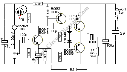
The output of this circuit is push-pull and consumes less than 3 mA (with no signal) but drives the earpiece to a very loud level when audio is detected. This circuit operates in a push-pull configuration, which allows it to...
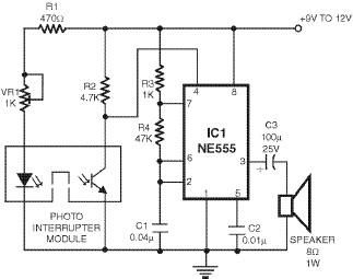
This smoke detector utilizes a 555 timer circuit along with common electronic components. The photo interrupter module serves as the smoke detection element, while the 555 timer is configured in astable mode to function as an audio frequency oscillator,...
The TV transmitter presented generates a stream containing four TV programs and broadcasts it on a frequency compliant with the DTT standard. It is suitable for integration into an antenna system and can utilize audiovisual channels generated on-site or...

Designing and implementing this circuit was an exciting endeavor. The design of the interface involved learning how to control a device from a computer. A parallel port cable was utilized for this purpose, enabling instant control of the stepper...
The target designator is designed based on the MSP430F149 microcontroller to facilitate rapid target identification in military training environments. It can adapt to various tactical requirements, allowing for the display of targets and the execution of bomb simulations according...
Power an RS232-TTL converter circuit using the serial port to eliminate the need for an external power supply. It has been noted that the DTR, RTS, and TD pins can facilitate this. Since the TD pin is already utilized...