
Using ADC 0808-ADC 0809 circuit chip consisting

The A/D conversion circuit employs the ADC0808 or ADC0809 integrated circuits, which are capable of converting an analog input voltage within the range of 0 to V (where V represents the maximum input voltage) into an 8-bit digital output. The ADC0808/ADC0809 chips are particularly suited for applications requiring high-speed conversions and are widely used in various electronic systems that need to process analog signals.
The operation of the A/D conversion circuit begins with the analog signal being fed into the ADC chip. The analog voltage is sampled and held by an internal sample-and-hold circuit, which stabilizes the input signal for accurate conversion. The ADC then quantizes the analog signal into discrete levels, corresponding to the 8-bit digital output. This means that the analog signal is divided into 256 distinct levels (2^8), allowing for a range of digital outputs from 00000000 to 11111111 in binary form.
The ADC0808 features a multiplexed input system, allowing multiple analog signals to be fed into a single ADC chip, while the ADC0809 includes a built-in comparator for applications requiring additional functionality. Both chips operate using a simple control interface, typically involving a clock signal and control lines to initiate the conversion process and read the output data.
The output from the ADC can be interfaced with microcontrollers or digital signal processors (DSPs), enabling further processing, analysis, or display of the converted data. This A/D conversion circuit is essential in applications such as data acquisition systems, audio processing, and sensor interfacing, where accurate digital representation of analog signals is crucial for system performance.A/D conversion circuit is to convert the analog voltage into a digital signal encoding circuit, is shown in FIG using ADC0808/ADC0809 circuit chips, which can be O ~ V convert analog signals into 8-bit digital output signal.
Related Circuits
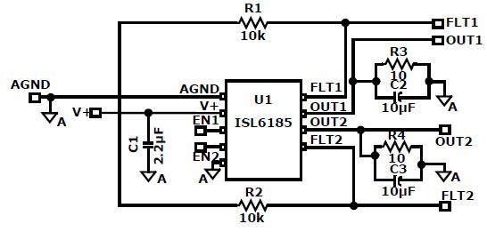
The ISL6185 USB power controller family can be utilized to design a straightforward USB power supply electronic project that offers fully independent overcurrent (OC) fault protection for two or more USB ports. This product family includes sixteen distinct functional...
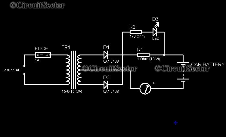
In today's world, owning a car battery charger at home has become essential. Having one readily available can help prevent starting issues caused by battery problems. While purchasing a commercial battery charger can be expensive, the components required for...
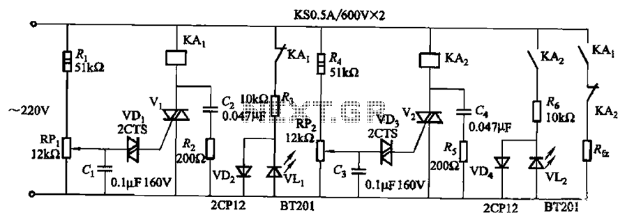
Bidirectional thyristor control. By adjusting potentiometers RPi and RPz, the lower and upper limit values can be changed. LEDs VLi and VL2 serve as indicators for low pressure and high pressure, respectively. The circuit utilizes a bidirectional thyristor to control...
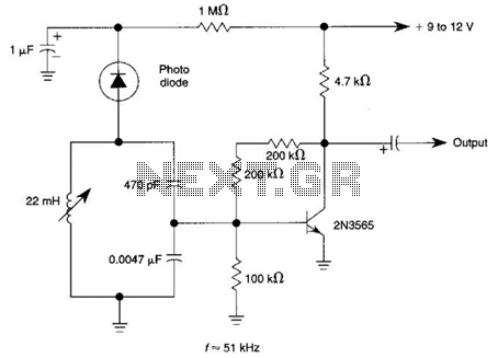
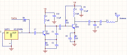
The circuit utilizes a tuned circuit for frequency selection, designed to operate at approximately 51 kHz. The 2N3565 transistor amplifies the output generated by the tuned circuit. The described circuit operates on the principle of resonance, where the tuned circuit...
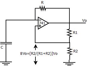
The positive feedback comparator circuit enhances the gain of the operational amplifier (op-amp), facilitating rapid switching between the two states of a multivibrator. This positive feedback also introduces hysteresis into the circuit. A capacitor, denoted as `C`, is connected...
This circuit utilizes a sawtooth oscillator along with an output amplifier that drives a transistor. The components C1, C2, and L1 are essential for the oscillator's operation, forming a tank circuit that must be tuned to the resonant frequency....