
Using DTMF encoding and decoding wireless calling implement circuit diagram

The wireless calling device operates by utilizing a dual-component architecture: the calling unit and the host. The calling unit is equipped with a DTMF (Dual-Tone Multi-Frequency) encoder, which is a critical component for generating the signaling tones necessary for communication. The DTMF encoder translates the input signals from the calling unit into specific frequency pairs that represent different digits or commands.
Each calling unit is designed with a unique code, allowing multiple units to operate within the same system without interference. This feature is essential for environments where multiple users may need to communicate with a single host unit simultaneously. Despite the unique codes, the underlying circuit design remains consistent across all calling units, promoting ease of manufacturing and maintenance.
The host unit receives the DTMF signals transmitted from the calling units. It is responsible for decoding these signals and executing the corresponding commands. The communication between the calling unit and the host is facilitated through a wireless protocol, ensuring flexibility and mobility for the user.
The use of a specific integrated circuit (IC2) for DTMF encoding ensures reliable performance and compatibility with standard telephone systems. This IC is capable of generating the necessary tones for both calling and signaling, enhancing the overall functionality of the device. The schematic of the calling unit, as referenced, illustrates the arrangement of components, including power supply connections, the DTMF encoder, and any additional circuitry required for signal transmission.
In summary, the wireless calling device's design emphasizes modularity, reliability, and user-friendliness, making it suitable for various applications where wireless communication is required. The integration of DTMF technology allows for efficient and effective signaling, contributing to the device's overall performance and utility.The wireless calling implement is composed of calling implement and the host. The two parts use DTMF encoder pulse to realise communication. Different calling implement has different codes only, the circuits are all the same. The calling implement is shown in figure 1. IC2 is the DTMF encoding specific integrated circuit (telephone dial tone can also be.. 🔗 External reference
Related Circuits
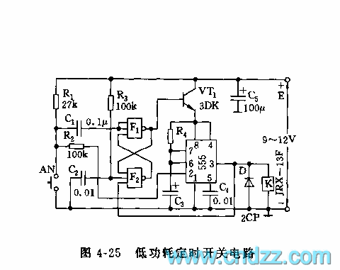
555 low power timing circuit diagram. The diagram is from the technical information of Chinaicmart. For more detailed information about the circuit diagram. The 555 timer IC is widely utilized in various applications due to its versatility and ease of...
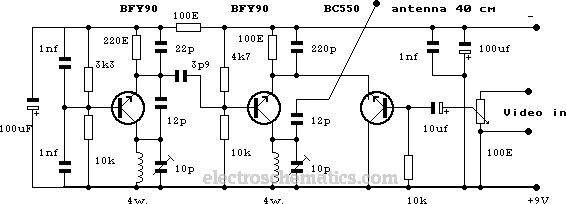
This compact video transmitter is highly effective for short-distance video surveillance, operating efficiently up to 100 meters. It can be paired with either a black-and-white or infrared camera module, providing excellent image quality on standard color or black-and-white televisions....
The current design of a power inverter offers an efficiency of approximately 85% and a power output exceeding 200 watts. This document provides a complete circuit schematic and detailed building procedure for a home-built power inverter. While numerous articles...
The ZN414 integrated circuit (IC) contains a complete automatic gain controlled AM receiver within a compact three-pin package. With only a few external components, it is possible to construct a simple radio that offers excellent selection and reception capabilities....
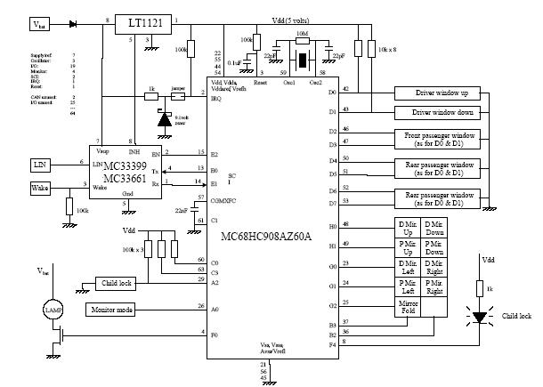
A car door differs from a calculator or a phone in that it makes sense to press more than one key at a time. The functionality of a car door can be compared to that of a multi-key input device,...
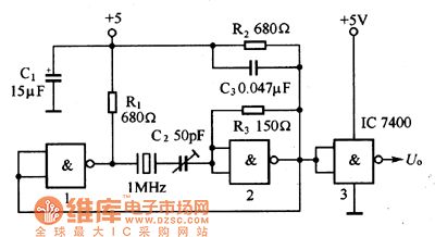
The oscillator circuit consists of a 1MHz quartz crystal resonator and a NAND gate, with the output buffer stage provided by NAND gate 3. This circuit can be utilized for calibrating standard frequency. The described oscillator circuit operates at a...