
Video Amplifier
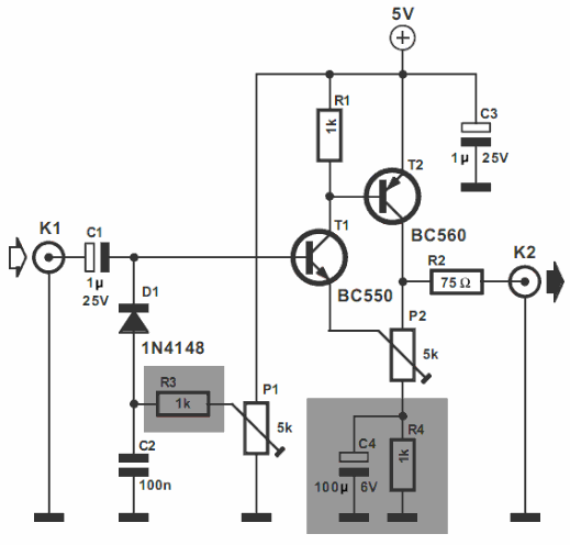
The video amplifier circuit operates by amplifying video signals for various applications. The design features two key potentiometers: P1, which adjusts the black level, and P2, which modulates the signal amplitude. The risk of transistor failure arises primarily from the potential for excessive current flow when these potentiometers are set to their extremes. Transistor T1 serves as the primary amplification stage, while T2 acts as a secondary stage for further signal processing.
To enhance the robustness of the circuit, resistors R3 and R4 are strategically placed to limit the base current entering T1 and T2, respectively. These resistors function as current limiters, ensuring that the base currents do not exceed 5 mA, thereby protecting the transistors from damage due to overcurrent conditions. The addition of these resistors not only safeguards the components but also contributes to the overall stability of the amplifier.
The shunt capacitor C4 plays a critical role in maintaining the performance of the amplifier. It is connected in parallel with R4 and serves to bypass high-frequency noise, ensuring that the amplification process remains unaffected by unwanted signals. This configuration allows for a cleaner output signal while preserving the integrity of the amplification process.
Overall, the video amplifier circuit exemplifies a balance between simplicity and functionality. The careful consideration of component placement and the inclusion of protective elements like resistors and capacitors contribute to a reliable and effective video amplification solution.The video amplifier in the diagram is a well-known design. Simple, yet very useful, were it not for the ease with which the transistors can be damaged if the potentiometers (black level and signal amplitude) are in their extreme position. Fortunately, this can be obviated by the addition of two resistors. If in the diagram R3 and R4 were direct co nnections, as in the original design, and P1 were fully clockwise and P2 fully anticlockwise, such a large base current would flow through T1 that this transistor would give up the ghost. Moreover, with the wiper of P2 at earth level, the base current of T2 would be dangerously high. Resistors R3 and R4 are sufficient protection against such mishaps, since they limit the base currents to a level of not more than 5 mA.
Shunt capacitor C4 prevents R4 having an adverse effect on the amplification. 🔗 External reference
Related Circuits

This is a preamplifier circuit and switching schematic for the Marantz Model 33. The Marantz Model 33 preamplifier circuit is designed to amplify low-level audio signals from various sources before sending them to a power amplifier. The schematic typically includes...
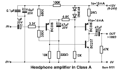
Even if simple, the circuit meets all conditions regarding distortion and frequency response. The input resistance is 250K ohms, and it can drive loads between 100 ohms and 2K ohms. The described circuit is a basic signal processing circuit designed...
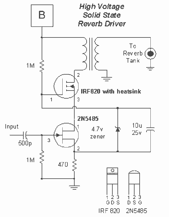
The IRF820 MOSFET has a voltage rating of 500V; it should work well in preamp stages of most tube amps. The 100-ohm resistor is there to suppress H.F. oscillations. If the IRF820 is physically close to the 12AX7 plate,...
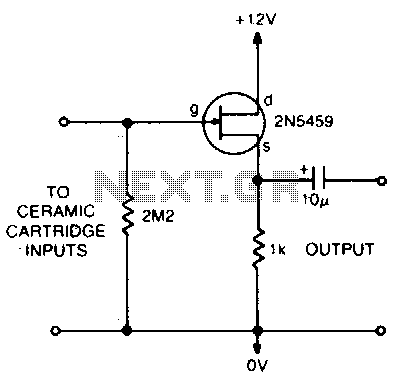
This circuit matches the very high impedance of ceramic cartridges, providing unity gain and low impedance output. By "loading" the cartridge with a 2.2MΩ input resistance, the cartridge characteristics are adjusted to closely compensate for the RIAA recording curve....
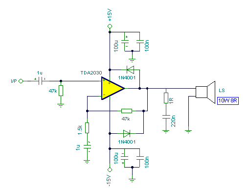
Connecting two TDA2030 through inexpensive power transistors allows for the creation of an amplifier capable of delivering higher power. This can be achieved by utilizing the component values specified in the schematic. To implement this circuit, two TDA2030 integrated circuits...
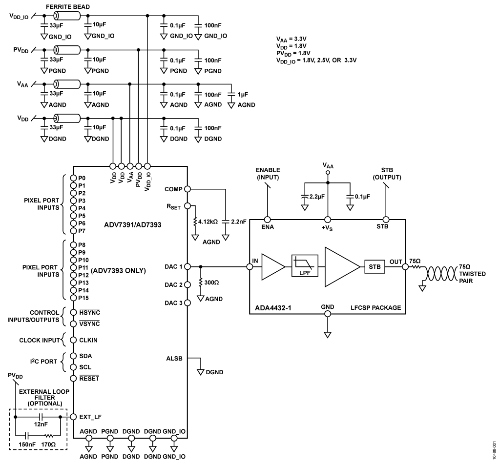
The ADV7390, ADV7391, ADV7392, and ADV7393 are a series of high-speed digital-to-analog video encoders integrated into single monolithic chips. Each chip features three 2.7 V/3.3 V 10-bit video digital-to-analog converters (DACs) that support composite (CVBS), S-Video (YC), and component...