
Video amplifier provides digital gain control
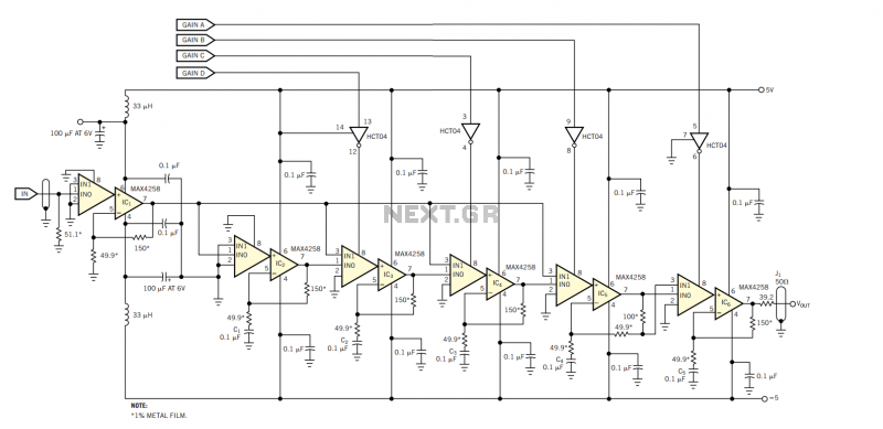
The amplifier circuit is designed to operate efficiently in environments with specific requirements, such as the Martian atmosphere. The use of Maxim MAX4258 dual-channel video multiplexer-amplifiers allows for flexible gain control through a 4-bit input word, enabling the user to adjust the gain stages dynamically. The architecture supports a configurable gain cascade, allowing for a total gain adjustment range of 36 dB, with each stage contributing an additional 12 dB.
The bandwidth characteristics of the amplifier are crucial, with each stage exceeding 100 MHz, providing a cumulative passband of over 60 MHz across all settings. The lowpass-bandpass capacitors (C1 to C5) play a significant role in defining the frequency response, specifically targeting the lower frequency range. A strategic choice of 0.1-µF capacitors ensures that the roll-off is maintained around 50 kHz, which is suitable for the intended application.
In terms of noise performance, the circuit achieves a low input-referred voltage noise level of approximately 2 nV/√Hz, which is comparable to the noise generated by a 250Ω resistor. This characteristic is vital for maintaining signal integrity, especially in high-gain settings. The inclusion of an HCT04 CMOS inverter in the gain-control pathway further enhances noise immunity, ensuring that control signals remain stable and free from interference.
The output specifications indicate a maximum output level of 15 dBm into a 50Ω load, which doubles for high-impedance loads, making the amplifier versatile for various applications. The design demands careful consideration of grounding and power supply bypassing to mitigate potential issues related to high-frequency operation and gain stability. Additionally, minimizing stray capacitance near the feedback components is essential to preserve the performance of the amplifier across its operational range.The amplifier in Figure 1 originally served as the photomultiplier preamplifier in a Doppler system intended for eventual operation in the Martian atmosphere. The design is based on a switchable array of six Maxim MAX4258 dual-channel video multiplexer-amplifiers, IC1 through IC6.
Under control of a 4-bit input word, you can set the number of stages in the gain cascade to three, four, five, or six. Because each multiplexer-amp has a fixed gain of four, each unit change in the stage count changes the overall gain by 12 dB.
In addition, you can interpose a 6-dB attenuator between the last and the next-to-last gain stages.
Gain-change settling time is lower than 30 nsec. The greater-than-100-MHz bandwidth of each stage results in an overall passband for all gain settings of greater than 60 MHz. The five lowpass-bandpass capacitors, C1 through C5, determine the lower end of the passband. In the original application, the frequencies of interest don't extend much below 100 kHz. So, using 0.1-µF capacitors results in a roll-off of approximately 50 kHz. Larger values for these capacitors would reduce this figure. Omitting the capacitors for a dc response is not recommended, however, because the resulting amplification of IC1's input offset would produce an output offset in the order of volts at high gain settings.
You can generate the gain-programming word using any TTL-compatible, 8-bit parallel-I/O port, such as a PC's parallel printer port or an EIA-1284-compatible port. The HCT04 CMOS inverter chip in the gain-control pathway blocks any possible noise entry in the gain-control lines.
The overall input-referred voltage noise is approximately 2 nV per the square root of hertz, equivalent to the Johnson noise of a 250W resistor. Maximum output level is 15 dBm (3.6V p-p) into 50W and twice that into high-impedance loads. The combination of extreme gain and high-frequency response (gain-bandwidth products approaching 200 GHz) of this circuit mandates careful attention to issues of ground-plane and power-supply-bypass integrity.
In addition, you must make every effort to minimize stray capacitance around the feedback-pin (Pin 5) components of all gain stages.
Related Circuits
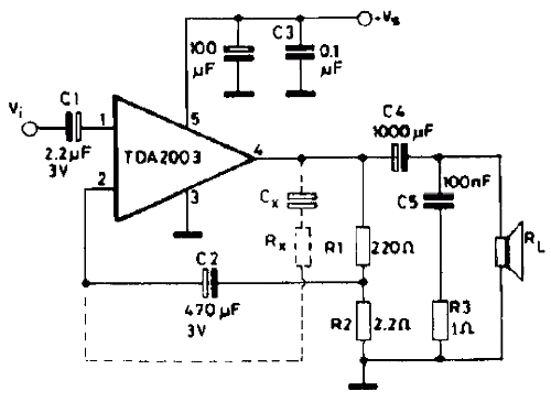
The TDA2003 offers enhanced performance while retaining the same pin configuration as the TDA2002. It maintains the advantageous features of the TDA2002, including a minimal number of external components, ease of assembly, and savings in both space and cost....
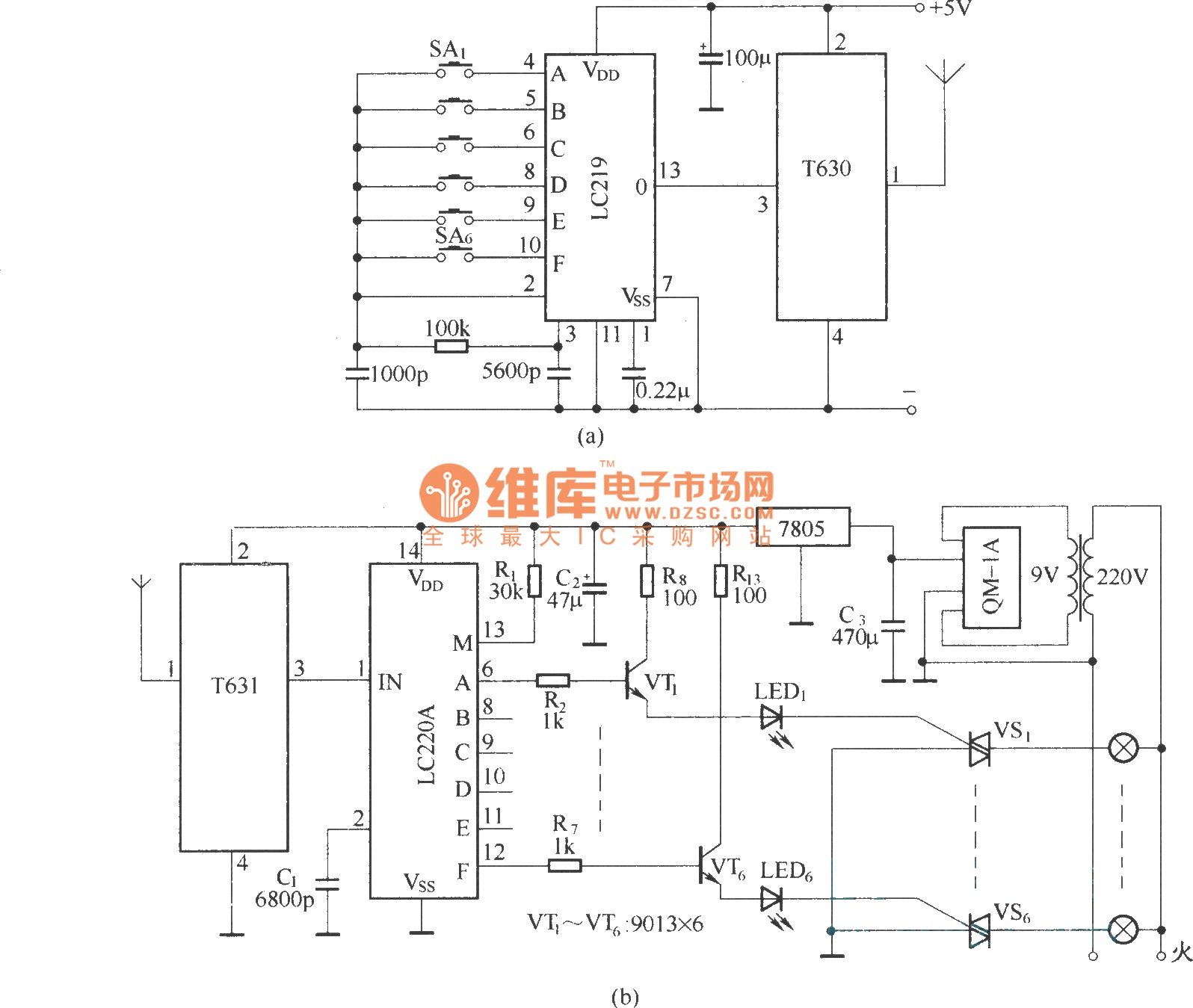
The circuit utilizes the long-wave wireless transceiver T630/T631 to manage a 6-channel load. It is characterized by low power consumption, high resistance to interference, and a simple structure. The circuit design incorporates the T630/T631 transceiver, which operates in the long-wave...
A stereo power amplifier is limited in its output power by two main factors - the impedance of the load and the internal power supply voltage. To obtain more power, one has very limited choices - other than the...
A circuit designed to extract and measure the modulated carrier signal from an infrared (IR) remote control. This circuit does not physically separate control pulses from modulation; instead, it amplifies the complete received signal, allowing the waveform to be...
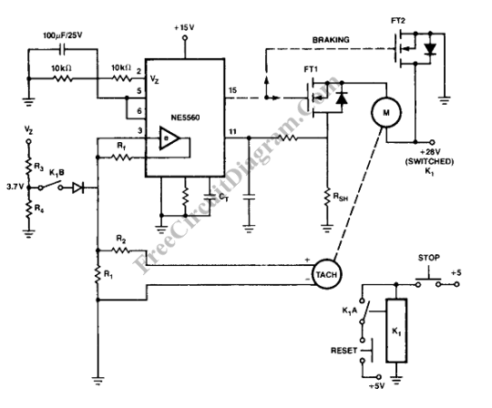
Closed loop motor control is utilized for maintaining constant speed in motor operations. This means that the motor's speed is regulated to remain steady. Closed loop motor control systems, commonly referred to as servo control systems, are essential in applications...
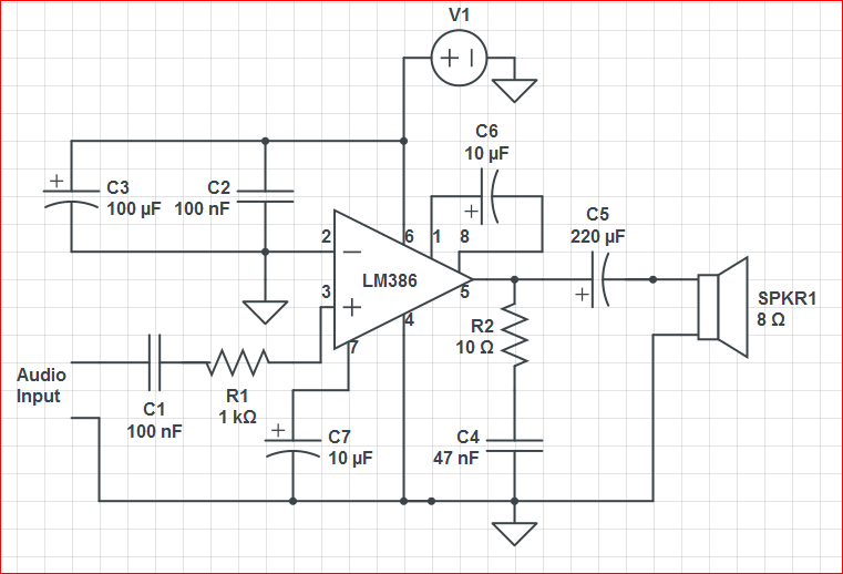
Initially, the circuit was connected to a 9V battery, which registered approximately 8.3 volts on a multimeter, within the operating voltage range for the LM386 as indicated in its datasheet. The output was characterized by significant noise, including crackling...