
Voltage follower with 1G ohm input resistances
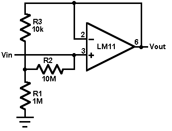
The described circuit employs the LM11 operational amplifier, a precision device known for its low offset voltage and high input impedance, making it suitable for applications requiring minimal signal distortion. The configuration as a voltage follower allows the circuit to maintain the input signal while providing high input resistance, which is essential when interfacing with high-impedance sources.
The use of a 1 GΩ resistor in conjunction with the LM11 ensures that the circuit does not load the signal source, preserving the integrity of the input signal. The input offset voltage, while typically small, can introduce errors in precision applications. By multiplying this offset by the feedback resistor R2, the circuit can account for this error, although the overall impact remains low due to the LM11's specifications.
When the input is connected to a source with a resistance lower than 1 GΩ, the error introduced by the input offset voltage is further minimized, enhancing the accuracy of the output signal. To accommodate AC signals, the addition of a 10 MΩ resistor in series with the inverting input is an effective strategy to mitigate bias current errors, which can otherwise distort the signal. This configuration allows for a more stable and reliable operation, particularly in sensitive applications.
If the series resistor is bypassed, the circuit remains functional with minimal noise, maintaining signal fidelity. This design approach is particularly advantageous in high-precision measurement systems, sensor applications, and any scenario where signal integrity is paramount. Overall, the circuit exemplifies a careful balance of component selection and configuration to achieve high performance in voltage follower applications.This circuit uses an LM11 to form a voltage follower with 1G ohm input resistance built using standard resistor values. With the input disconnected, the input offset voltage is multiplied by the same factor as R2; but the added error is small because the offset voltage of the LM11 is so low.
When the input is connected to a source less than 1G ohm , this error is reduced. For an ac-coupled input a second 10M resistor could be connected in series with the inverting input to virtually eliminate bias current error; bypassing it would give minimal noise. 🔗 External reference
Related Circuits
This article presents a high reliability 1200V High Voltage Integrated Circuit (1200V HVIC) for half bridge driver applications, aimed at reducing the IC's supply current by approximately 50%. The 1200V High Voltage Integrated Circuit (HVIC) is designed specifically for half-bridge...
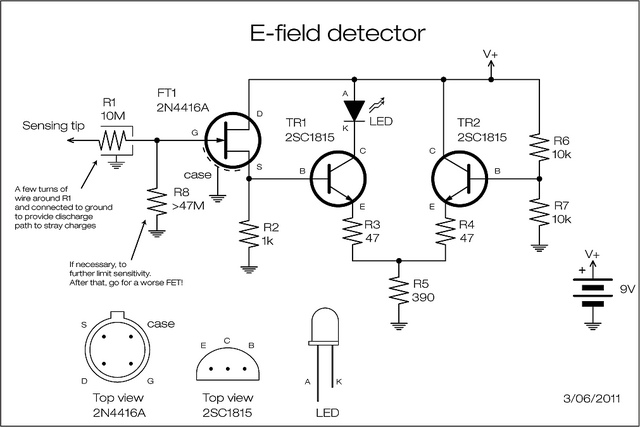
A JFET is employed to detect the electric field generated by high voltage power lines. The JFET amplifies the signal minimally but reduces the impedance and supplies current at a level appropriate for transistor amplification. The two transistors can...
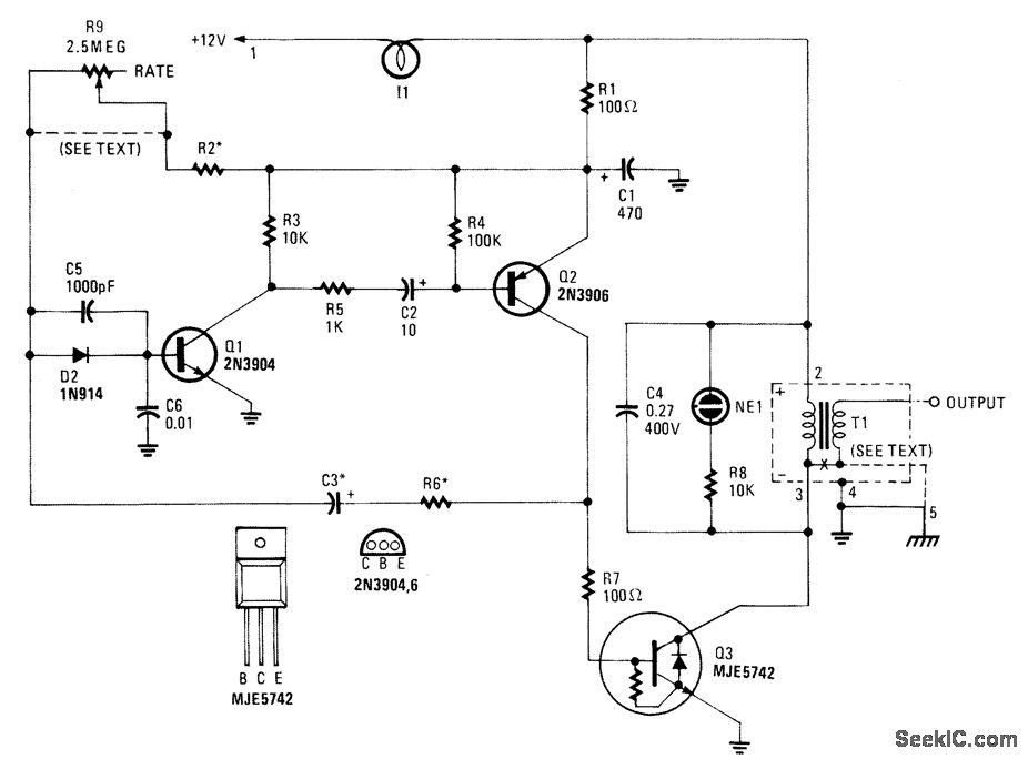
This high-voltage pulse supply generates pulses up to 30 kV. Transistors Q1 and Q2 create a multivibrator in conjunction with peripheral components R1 through R6 and capacitors C1, C2, C3, C5, C6, and diode D2. Resistor R9 adjusts the...
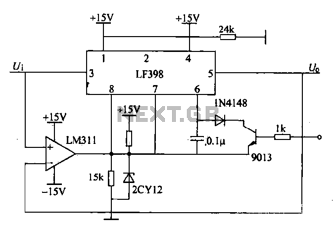
The peak voltage sample and hold circuit is illustrated in Figure 12-50. This circuit comprises the LF398 sample and hold chip and the LM311 voltage comparator. The LF398 is responsible for outputting and inputting voltages. The LM311 compares the...
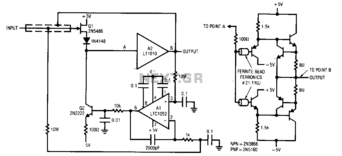
Q1 and Q2 form a simple, high-speed FET input buffer. Q1 operates as a source follower, while Q2 serves as a current-source load that regulates the drain-source channel current. The LT1010 buffer is utilized to provide output drive capability...
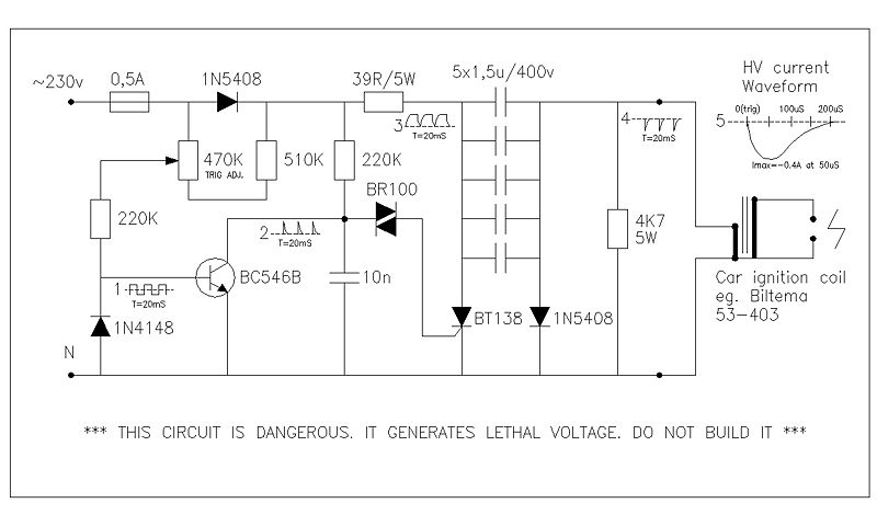
This circuit generates high voltage pulses from a 230 VAC line voltage. The drive end's swing comparator circuit was developed by the creator of this page. The working end is derived from a stroboscope trigger supply circuit. All circuits...
Warning: include(partials/cookie-banner.php): Failed to open stream: Permission denied in /var/www/html/nextgr/view-circuit.php on line 713
Warning: include(): Failed opening 'partials/cookie-banner.php' for inclusion (include_path='.:/usr/share/php') in /var/www/html/nextgr/view-circuit.php on line 713