
VOLTAGE SHIFTING CIRCUIT DIAGRAM

The described circuit is designed to modify the output voltage range of a Digital-to-Analog Converter (DAC). This functionality is crucial in applications where the DAC output needs to be adjusted to fit the input requirements of subsequent stages, such as power operational amplifiers (op-amps). The schematic typically includes the DAC, which generates a voltage based on a digital input signal, and additional components that facilitate the voltage shifting process.
The voltage shifting mechanism may involve operational amplifiers configured in various configurations, such as inverting or non-inverting amplifiers, to achieve the desired gain and offset adjustments. Feedback resistors are commonly used to set the gain, while additional resistors may be employed to create a reference voltage that establishes the output range.
The output from the DAC is fed into the input pins of the power op-amps, which amplify the signal to a level suitable for driving loads or interfacing with other circuit elements. Proper consideration must be given to the power supply requirements of the op-amps to ensure they operate within their specified ranges.
Overall, the circuit's design emphasizes the importance of accurate voltage shifting to ensure compatibility with downstream components, thereby enhancing the overall performance and reliability of the electronic system.As mentioned in the chapter about the DAC, this circuit shifts the voltage output range. The following diagram explains it's operation and structure. The circuits outputs are connected to the input pins of the power opamps. 🔗 External reference
Related Circuits
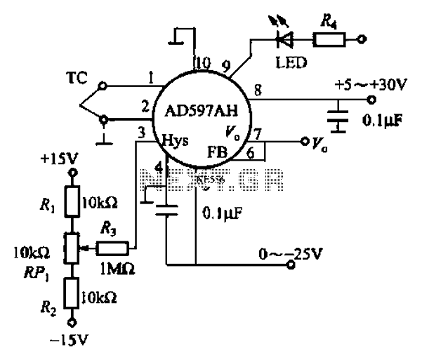
An automatic electric furnace temperature controller is illustrated. The closed circuit consists of a temperature detection output control loop; as the temperature increases, the output voltage rises until it reaches a preset temperature value, at which point the output...
This circuit is representative of the typical application of a photomultiplier tube. The circuit depicted is AC coupled; however, if DC coupling is required, the capacitor can be removed, and an appropriate interfacing method should be employed. A common...

ECL integrated circuit non-saturated digital logic circuits. CMOS and ECL interface circuit shown in cross. ECL (Emitter Coupled Logic) integrated circuits are designed to operate in a non-saturated mode, providing high-speed digital logic functionality. These circuits are characterized by their...
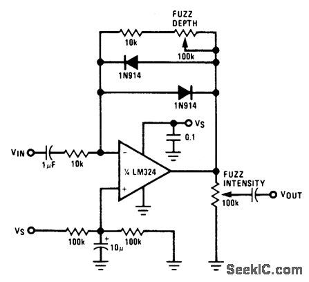
Two diodes in the feedback path of an LM324 operational amplifier create a musical instrument effect known as fuzz by limiting the output voltage swing to ±0.7 V. The resultant square wave primarily contains odd harmonics, resembling the sounds...
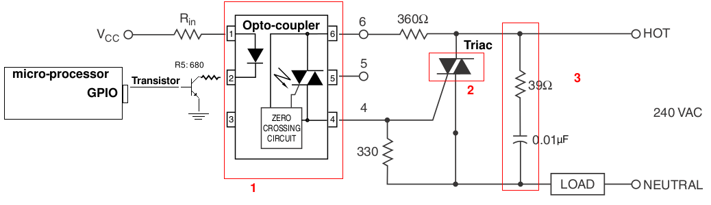
A light-dimming control system is being developed for a 240V heat lamp with a power dissipation of approximately 250W. The objective is to adjust the heat output of the lamp using control from a microprocessor. The development is based...
After charging the batteries for many hours with the 12V charger and PowerCheqs, a drive of about 5 miles resulted in the low battery light activating. The PakTrakr indicated that the battery adjacent to the most positive battery required...