
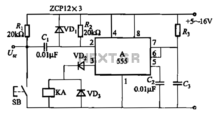
Voltage-To-Frequency Converter (VFC) with 555 IC
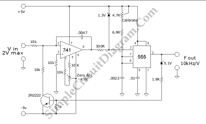
The voltage-to-frequency converter is a crucial component in various analog and digital applications, converting an input voltage level into a corresponding frequency output. The primary function of a VFC is to provide a frequency signal that can be easily processed by digital systems, such as microcontrollers or frequency counters.
The circuit typically includes a 555 timer IC configured in astable mode. In this configuration, the 555 timer generates a continuous square wave output whose frequency is determined by the input voltage and the timing components, which usually consist of resistors and capacitors. The relationship between the input voltage and the output frequency can be described by the formula:
\[ f = \frac{1.44}{(R1 + 2R2)C} \]
Where:
- \( f \) is the output frequency,
- \( R1 \) and \( R2 \) are the resistances connected to the 555 timer,
- \( C \) is the capacitance of the timing capacitor.
In the schematic, the input voltage is applied to the control voltage pin of the 555 timer, allowing it to modulate the output frequency based on the input voltage level. Additional components may include diodes for protection against reverse polarity, potentiometers for fine-tuning resistance values, and bypass capacitors to stabilize the power supply.
The output frequency can be monitored using an oscilloscope or a frequency counter, making this circuit suitable for applications such as sensor interfacing, signal conditioning, and data acquisition systems. The design is compact and can be easily integrated into larger systems, providing a versatile solution for converting voltage levels to frequency signals.Voltage-to-frequency converter (VFC)? circuit is shown in the schematic diagram below. The circuit employs 555 IC as the core of its function. This circuit . 🔗 External reference
Related Circuits
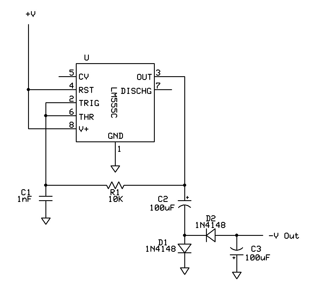
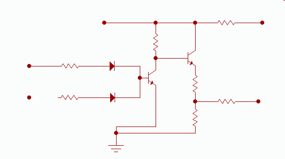
Can a 555 negative supply circuit, like the one below I pulled from another schematic, supply enough negative voltage to an LM324 and an AD736JN? The 555 timer integrated circuit can be configured to generate a negative voltage supply,...
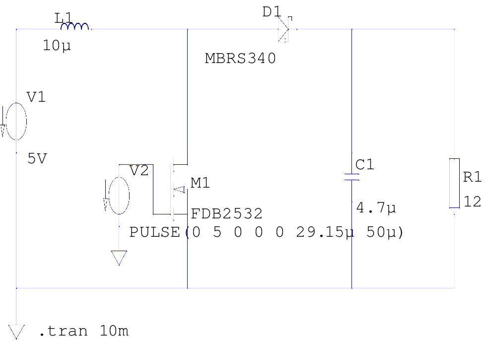
The supply voltage is 5V, and the goal is to increase it to 12V with a load current of 1A, resulting in an output power of 12W. A switching frequency of 20kHz has been selected, requiring a duty cycle...
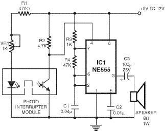
This smoke detector utilizes a 555 timer circuit along with common electronic components. The photo interrupter module serves as the smoke detection element, while the 555 timer is configured in astable mode to function as an audio frequency oscillator,...
I realized the first schematic shown here, because it's more simple, but I took all information about the other pins from the second schematic. Be careful with all connections and control everything more than once to ensure the circuit...
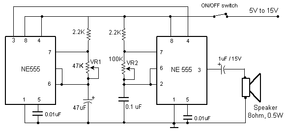
This circuit produces the sound of a beeper like the one in pagers which produces a "beep-beep" sound. Basically the circuit consists of a 555 timer oscillator which is turned ON and OFF periodically. The first IC (left) oscillates...
The 555 integrated circuit is utilized in a delay circuit configuration, functioning as a one-shot timer. The delay time can be adjusted using resistor R3 and capacitor C3. Typical values for R3 range from 1 kΩ to 10 MΩ,...