
Wide band 10MHz 500MHz RF amplifier
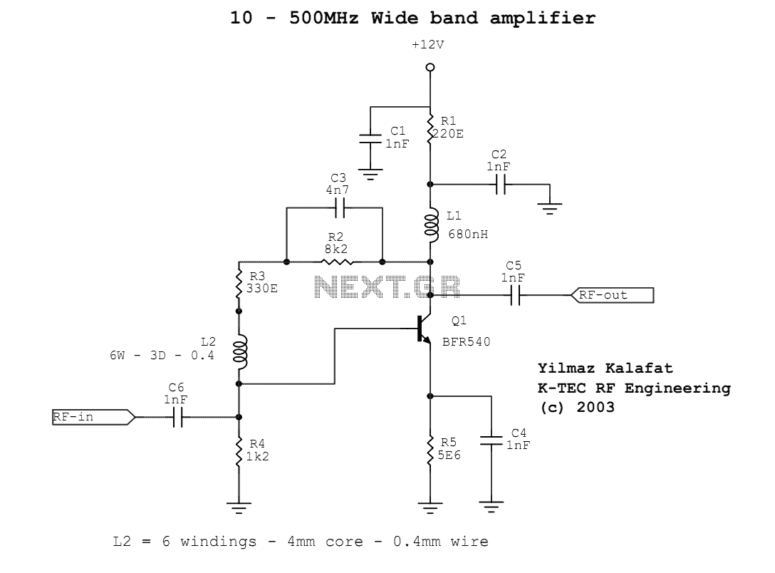
The RF amplifier circuit described operates effectively within a frequency range of 10 MHz to 500 MHz, classifying it as a wideband amplifier. This type of amplifier is integral to various applications, including communication receivers and RF measurement devices. The design incorporates a high-performance transistor capable of operating at frequencies up to 9 GHz, ensuring optimal performance across the specified frequency range.
The circuit's gain is primarily controlled by feedback resistors R2 and R3. Adjusting the resistance values allows for increased gain at lower frequencies; however, this adjustment may adversely affect the amplifier's overall gain profile. The inclusion of coil L2 enhances gain at higher frequencies, but caution is warranted, as increasing its value may lead to instability in the circuit. The coil is specified to have six windings, an inner diameter of 3 mm, and a wire thickness of 0.4 mm, which are critical parameters for maintaining performance.
For the prototype stage, a surface-mount device (SMD) type inductor was utilized for L1, emphasizing the need for a high-quality (high Q) coil to minimize losses and enhance overall efficiency. The circuit is designed with the principle of maintaining short connections to reduce parasitic capacitance and inductance, which is vital in RF applications.
The amplifier operates with a supply voltage of +12V and a current consumption of 10 mA. It has an input and output impedance of 50 Ohms, which is standard for RF applications to ensure maximum power transfer and minimize reflections. The noise figure of the amplifier is typically 3.5 dB, indicating good performance in terms of signal clarity. Additionally, the circuit boasts an input intercept point (IP2) of 110 dBuV and an output intercept point (IP3) of 105 dBuV, which are critical metrics for assessing the linearity and dynamic range of the amplifier.This paper describes an RF amplifier circuit which is suitable for the frequencies between 10MHz and 500MHz. These kind of amplifiers are called wide band amplifiers. Wide band amplifiers are used in communication receivers, RF measuring equipment and tons of other devices.
The circuit described here uses a state of the art transistor to get maximum performance at high frequencies. It can be used as a low noise pre-amplifier due to his low noise characteristics. This is a classical RF amplifier design. The feedback resistors R3 and R2 define the gain. By changing the values we can get a higher gain at low frequencies, but this will influence the overall gain taper of the amplifier. Coil L2 is used to get more gain at high frequencies. If the value is increased, instability will occur. Dimensions of L2 are: 6 windings, inner diameter is 3mm and wire thickness must be 0.4mm. In the proto type I used and SMD type for L1, make sure it’s a high Q coil. The transistor, which is used here, is a wide band transistor with an Ft of 9 GHz. Like in all other RF circuits make sure that the connections are short as possible. Supply voltage : +12V Current : 10mA Input / output impedance : 50 Ohm Frequency range : 10MHz 500MHz Noise figure : 3.5dB typical IP2 : 110dBuV IP3 : 105dBuV
🔗 External reference
Related Circuits
The supply voltage should be about +/- 35 Volts at full load, which will let this little guy provide a maximum of 56 Watts (rated minimum output at 25 degrees C). To enable maximum power, it is important to...
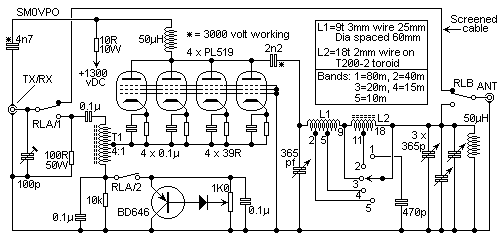
This is the circuit of a 500 watt linear amplifier, based upon a design by Frits Geerligs, PA0FRI. The circuit uses four PL519 TV line output valves in a very simple circuit that will deliver over 450 watts at...

This circuit is a graphic equalizer that can be built with a low component count and is controlled using the LA3600 single IC chip. The internal design of the chip utilizes a transistor gyrator circuit, with connections to external...
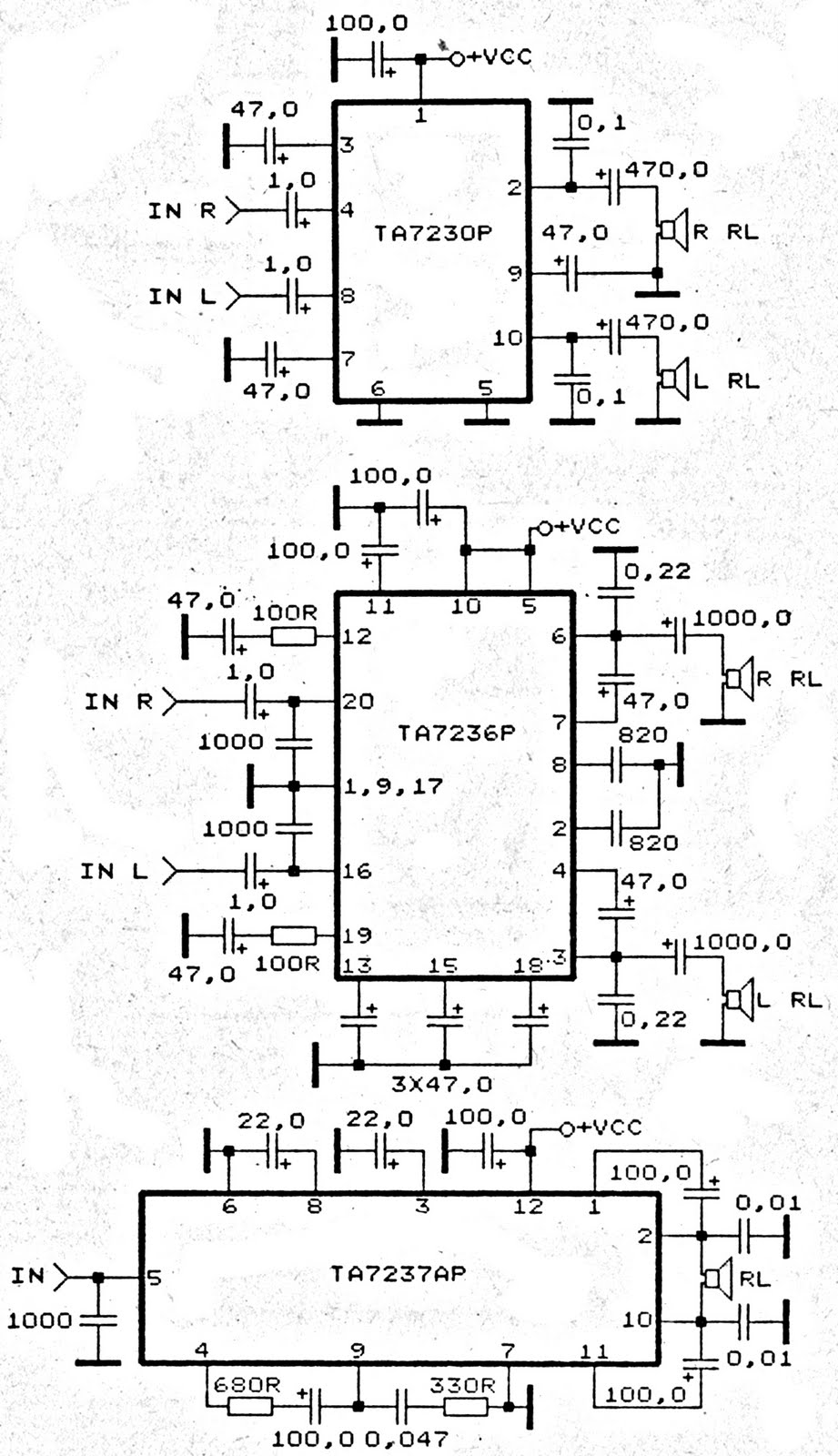
The amplifier circuit is based on integrated circuits (ICs) that determine the gain. Three specific ICs, TA7230P, TA7236P, and TA7237AP, are utilized as power amplifiers. Each IC has distinct output characteristics and input voltage requirements. All three ICs are...
This is a 25-watt basic power amplifier designed for ease of construction at a reasonable cost. It outperforms the standard STK module amplifiers commonly found in mass-market stereo receivers today. The design was initiated to create a 25-watt amplifier...
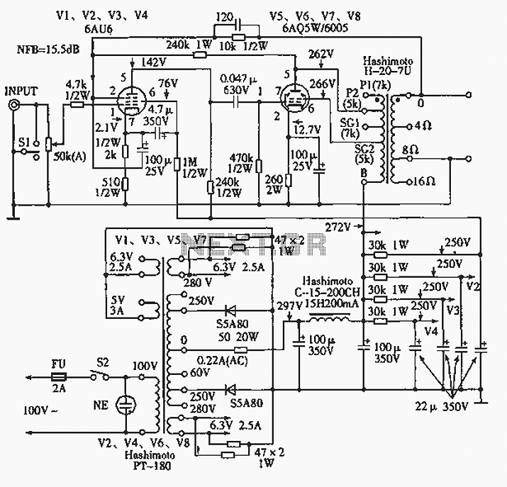
The 6AQ5W / 6005UL four-channel single-ended amplifier circuit is illustrated in the accompanying figure. Only two channels are shown, but it is part of a four-channel system that employs a power transformer for the voltage amplification section. This section...
Warning: include(partials/cookie-banner.php): Failed to open stream: Permission denied in /var/www/html/nextgr/view-circuit.php on line 713
Warning: include(): Failed opening 'partials/cookie-banner.php' for inclusion (include_path='.:/usr/share/php') in /var/www/html/nextgr/view-circuit.php on line 713