
Wide band power detector to control microwave station
The calibration process involves introducing a known level at the RF input and inputting this level into the microcontroller to correct measurement errors. Several points are necessary for effective correction, which are frequency-dependent. The calibration algorithm determines the best linear regression to minimize errors across the entire dynamic range. This process is conducted using an external test bench that includes an RF synthesizer and a commercial power meter, taking approximately 50 data points of Vdetected as a function of Pin, and calculating the gain and offset for each frequency. These values are stored in ROM. The calibration accounts for the linearity error of the detector and the imperfections of the input attenuator, with measurements displayed directly in dBm.
For the proposed kit, two types of calibration are possible: the default standard calibration (kit#1 and kit#2) offers an accuracy of approximately ±0.5 dB up to 1.2 GHz and about ±1 dB for higher frequencies. A dedicated calibration for the DetLog board, tested only on kit#3, achieves an accuracy of around ±0.2 dB. It is important to note that the calibration algorithm does not operate across the frequency axis, meaning that no correction occurs between two calibrated frequencies. For instance, to measure at 3400 MHz, one would need to use the nearest calibration, such as at 2320 MHz, resulting in suboptimal correction. A built-in calibration process can be executed at 3400 MHz to calculate linearization parameters for this frequency, which can then be stored in available memory.
The built-in calibration utilizes up to eight measurement points to calculate linearization, and this procedure can also accommodate external attenuators or coupling factors. Upon completion of the calibration process, the parameters are saved into the current calibration memory located in ROM, which retains data even after power-off. A total of nine memory banks are available for saving calibration data for future use.
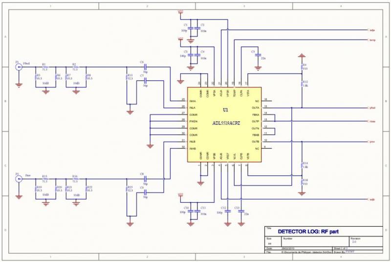
This comprehensive calibration and measurement system ensures accurate power measurement and reflects the robustness of the ADL5519 in various applications, particularly in high-frequency environments.The particular interest of the ADL5519 is focused on bandwidth which is specified up to 8GHz (but still usable in 10GHz with reduced dynamic). With two channels, it is possible to measure the power transmitted to the antenna and the reflected wave, to calculate the return loss and block the PTT when problems arise.
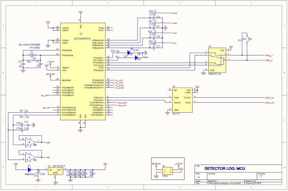
As I originally destined it to my EME 13cm station the module is controlled remotely by serial interface (RS232 and RS485) to be installed in the antenna 30m away the shack. A simple RS232 VT100 terminal allows the full control of the assembly as the whole software is embedded.
The set also includes some additional features such as measuring the temperature of the PA with KTY probes and power supply voltages. The calibration process is the action of putting a well known level at the RF input and entry this level to the microcontroller to correct the measurement error. Of course few points are necessary to obtain good correction and those are frequency dependant. The calibration algorithm finds then the best linear regression minimizing the error over the full dynamic.
This process is done by an external test bench based on RF synthesizer and commercial power meter, taking about 50 points Vdetected = f (Pin), and calculating the gain and offset for each frequency. These values are then stored in ROM. The calibration takes into account the linearity error of the detector and the imperfection of input attenuator.
The measurement is then displayed directly in dBm. Basically for the kit proposed below two calibration are possible: . Default standard cal (kit#1 and kit#2) accuracy around typ. +/-0.5dB up to 1.2G and typ +/- 1dB for higher freq. . Calibration dedicated to the DetLog board mounted and tested only possible on kit#3. Then the accuracy is around +/- 0.2dB Remark: The calibration algorithm does not work on the frequency axis. It means that between two calibrated frequencies no correction is done. Example: If you want to measure at 3400 MHz you have to use the closer cal, let say 2320 MHz and then correction is not optimal.
You could run the built in calibration process at 3400 MHz to calculate the linearization parameters at this frequency and save it on one free memory. The built in cal use up to 8 measurements points to calculate the linearization. This procedure can also be used to take into account external attenuator or coupling factor. At the end of the process the cal parameters are saved into the current cal memory which is located in ROM (no volatile after power off).
A total of 9 memory banks are available to save calibration for further uses. 🔗 External reference
Related Circuits
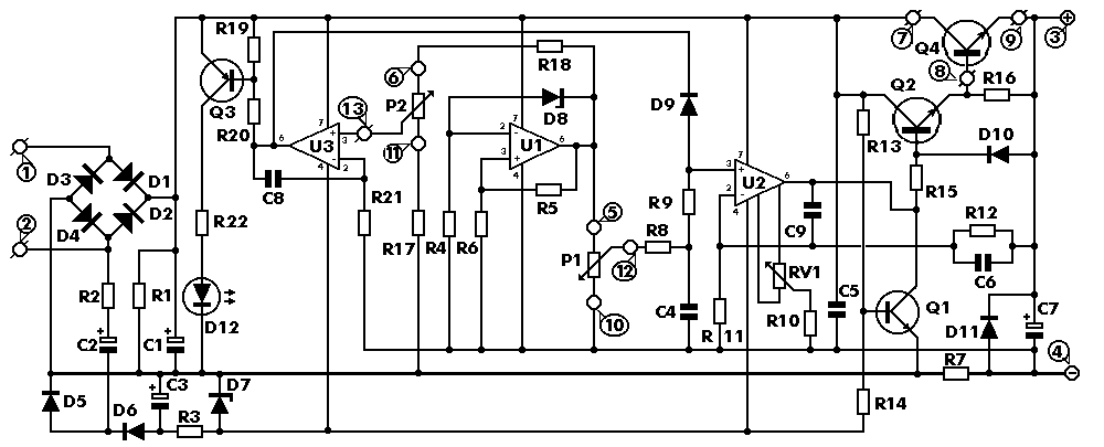
This is a high quality power supply with a continuously variable stabilised output adjustable at any value between 0 and 30VDC. The circuit also incorporates an electronic output current limiter that effectively controls the output current from a few...
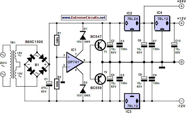
Inexpensive miniature transformers typically provide one or two secondary voltages, which are sufficient for generating a set of positive and negative supply voltages, as required for operational amplifier circuits. However, if an additional voltage higher than either of the...
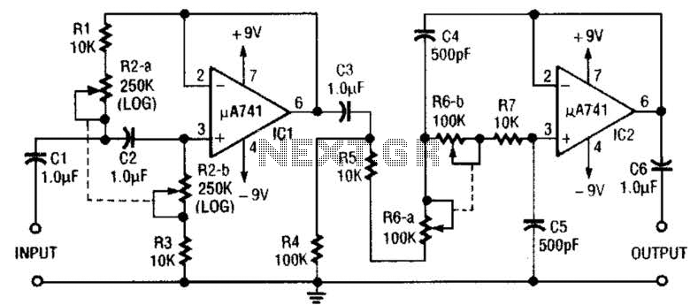
This circuit is a variable audio bandpass filter that features a low cutoff adjustable from approximately 25 Hz to 700 Hz and a high cutoff adjustable from 2.5 kHz to over 20 kHz. The roll-off is set at 12...
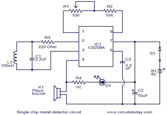
This is a simple single-chip metal detector circuit based on the IC CS209A from Cherry Semiconductors. A 100µH coil is utilized to detect the presence of metal. The IC CS209A incorporates a built-in oscillator circuit, with the coil (L1)...
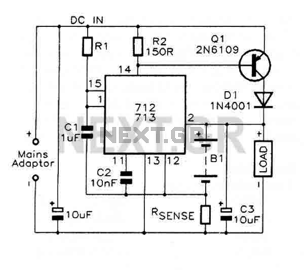
The MAX712 and MAX713 are nickel cadmium (Ni-Cd) battery fast charge controllers that facilitate the rapid charging of batteries from a DC source, which must be at least 1V higher than the maximum battery voltage. These controllers can charge...
This document explains a simple circuit designed to remotely switch on or off any electrical device using a relay, controlled by a standard TV or VCR. The circuit utilizes a relay as the primary switching element, enabling the control of...
Warning: include(partials/cookie-banner.php): Failed to open stream: Permission denied in /var/www/html/nextgr/view-circuit.php on line 713
Warning: include(): Failed opening 'partials/cookie-banner.php' for inclusion (include_path='.:/usr/share/php') in /var/www/html/nextgr/view-circuit.php on line 713