
Wiper control circuit IIV

The circuit utilizes a timer IC (U1), typically a 555 timer, configured in astable mode to create a continuous square wave output. This mode is characterized by the timer oscillating between its high and low states, effectively functioning as a relaxation oscillator. The charging and discharging of capacitor C2 dictate the timing intervals of the output signal. Resistors R1, R2, and R3 form a voltage divider that influences the charge and discharge rates of C2, thus controlling the frequency of oscillation.
Initially, when power is applied, C2 begins to charge through the resistors, reaching two-thirds of the supply voltage. At this voltage level, U1's internal comparator at pin 6 triggers, resulting in a high output at pin 3. This output is crucial as it prevents Q1 from conducting, keeping the relay K1 de-energized. The discharge of C2 occurs through R2 to pin 7 of U1, and once the voltage across C2 drops to one-third of the supply voltage, the timer resets, toggling the output state.
The subsequent low output at pin 3 activates Q1, which acts as a buffer to drive the relay coil. As Q1 turns on, it allows current to flow through the coil of relay K1, closing the contacts and energizing the connected load, such as wipers in an automotive application. The timing characteristics of the circuit can be adjusted by varying R3, allowing for customization of the on and off durations of the output signal. The choice of tantalum capacitor C2 is important due to its stability and reliability under varying conditions, while the relay should be selected based on the load requirements to ensure adequate performance.U1 is configured to operate in the standard astable mode, providing a form of relaxation oscillator. When power is applied, C2 initially charges through Rl, R2 and R3 to two-thirds of the supply voltage. At that point, U1 senses that its threshold voltage at pin 6 has been reached, and triggers the timer, causing its output at pin 3 to go high.
That high, applied to the base of Ql, keeps the transistor in the off state. Now C2 begins to discharge through R2 to pin 7 of Ul. When C2 has discharged to about one-third of the supply voltage, Ul is toggled back to its original state. C2 starts to charge again, as pin 3 of Ul goes low. The low at pin 3 causes Ql—which serves as an emitter-follower buffer stage—to turn on, allowing current to flow through the coil of relay Kl. That, in turn, causes Kl's contacts to close, applying power to the wipers. The charge time of capacitor C2 is determined by the setting of potentiometer R3. Capacitor C2 should be a tantalum type, and actually, almost any 12-volt coil relay with sufficiently heavy contacts should serve well.
Related Circuits
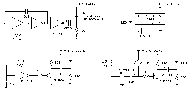
The LED flasher circuits below operate on a single 1.5 volt battery. The circuit on the upper right uses the popular LM3909 LED flasher IC and requires only a timing capacitor and LED. The top left circuit, designed by...

This is the design circuit diagram of an ultrasonic mosquito repeller. The circuit operates based on the theory that insects, such as mosquitoes, can be repelled by sound frequencies in the ultrasonic range (above 20 kHz). The circuit utilizes...
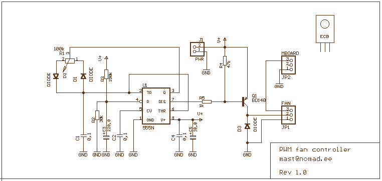
This 555 timer based PWM controller features almost 0..100% pulse width regulation using R1, while keeping the oscillator frequency relatively stable. The frequency is dependent on values of R1 and C1, values shown will give a frequency range from...
This circuit design generates a stable 1 kHz sine wave using an inverted Wien bridge configuration with components C1-R3 and C2-R4. It offers a variable output, low distortion, and low output impedance to ensure good overload capability. The circuit...
Its state is constantly changing, and this change affects the flow of current and voltage, which is visible with the two LEDs. The speed of the LED flasher can be adjusted with potentiometer P1. As an astable multivibrator, the...
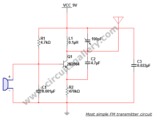
This is the simplest single transistor FM wireless transmitter circuit ever posted in CircuitsGallery. In the field of telecommunications, frequency modulation (FM) transmits information by altering the frequency of a carrier wave based on the message signal. FM utilizes...