
With a CD4011 dual-produced sound and light control delay lamp circuit
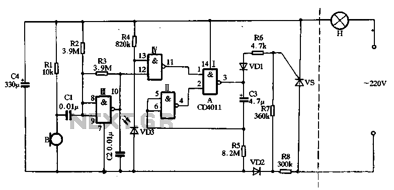
When the AC power is in the positive half-cycle, the SCR remains off. The AC current is converted to a DC source through the VD2 half-wave rectifier. During the negative half-cycle, resistors R8 and R7 provide trigger current, but the output at pin 3 remains low, preventing the lamp from lighting. When the microphone detects an acoustic signal, the corresponding electrical signal is coupled to the input of NAND gate III (pins 8 and 9), amplifying the signal at pin 10. If the peak value of the audio signal exceeds the threshold of NAND gate II, it flips to output logic "0," which sets the output of NAND gate I to logic "1," turning on the lamp.
As the output at pin 3 is high, it charges the coupling capacitor (C3) through resistor R5, causing the voltage across C3 to rise. This results in a decrease in the input level at pins 5 and 6 of NAND gate I. Once the input level falls below the threshold, the output at pin 4 switches to logic "1." If there are no further sounds in the environment, the output at pin 3 returns to logic "0," turning off the SCR and extinguishing the lamp. The duration of the lamp's illumination is primarily determined by the time constant of R5 and C3. A photodiode (VD3) is incorporated into the light control circuit, providing high resistance at night, thus allowing pin 13 to remain high (logic "1"). Conversely, during the day, VD3 exhibits low resistance, making pin 13 a logic "0," which prevents the lamp from being activated by environmental sounds.
The circuit design effectively integrates various components to control the operation of the lamp based on ambient sound levels and light conditions. The use of NAND gates allows for efficient signal processing, while the combination of resistors, capacitors, and diodes ensures that the circuit responds appropriately to both sound and light inputs. This design can be applied in various applications, such as automatic lighting systems that respond to environmental changes. The careful selection of component values will influence the sensitivity and response time of the circuit, allowing for customization based on specific requirements.The main circuit uses a two-input NAND gate four digital integrated circuits, wherein the composition of NAND gate III microphone amplifier circuit; NAND gate t composition and the amplified signal light control "and gate" Control i NAND gate and NAND I gate II composition monostable delay control circuit. The entire circuit is powered by a resistor R8 buck, VD2 half-wave rectifier, filter capacitor C4 is supplied with.
Static, with the input of the NAND gate I due R2 connected to the positive power supply, so the output of lo pin is low, NAND gate t12 foot logic "O" so whether l3 feet daytime logic "O" or night logic "1", its output pin 11 always lose out logic "1." II logic input NAND gate terminal 5,6 feet "0", the output terminal 4-pin output logic "1", so this time I NAND gate of two inputs l, 2 feet are logic "l", 3 is a logic output terminal "O". When the AC power is positive half cycle (ie, the positive negative), the SCR vs non-conducting condition off, then AC by VD2 half-wave rectifier circuit to provide electrical source.
When a negative half-cycle alternating current (ie, the negative in positive), the resistance R8, R7 series vs provide for the trigger current, static due to the 3-pin output logic state "O", the forward current through R7, R6, VD1 and NAND gate I 3 feet into the ground, vs gate at a low level, vs off, so H lamp does not light. When B receives the microphone after the acoustic signal environment corresponding output electrical signal, this signal is cl coupled to the NAND gate III after input of 8,9 feet, amplifying the signal output from the IO pins.
When the positive half cycle peak value of the audio signal exceeds the NAND gate t Min value level, the NAND gate t flip. II pin output logic "0" (set at this dark environment, 13 feet for the logic level "1"), so I NAND gate 3 feet output logic "l", a diode VDI off, vs will get triggered by R7 current opening of the lamp H lights up.
At the same time, 3 feet high by making the input coupling capacitor C3 NAND II 5,6 two feet high, so the output 4-pin output logic "O", and added directly to the NAND gate I 2 feet. At this point even the 10 foot level changes occurred with the audio already, so I NAND gate 1 at logical "l", but due to 2 feet for a logic "O" on the insurance certificate of the 3-pin output logic "l", H still so light stays on.
In light while high by 3 feet on to charge the capacitor C3 R5, the voltage across the capacitor rising. Therefore, NAND gate I1 input of 5,6 feet level constantly decreases, when the level is below the threshold input NAND gate, four feet will output logic "l", at this time if the environment is no longer sound, 1 pin for logic "l", the 3-pin output logic "O", SCR vs off, light H goes out.
If the ambient sound again, the lamp can be lit again. The duration of the lighting lamp is mainly determined by R5 and C3 of the charging time constant. R4 and photodiode light control circuit VD3 composition night VD3 showed high resistance, so that 13 feet high "l", which with the output of NAND gate t II foot level when the level depends only on the level change of 12 feet , that depends only on whether the ring Tu sound decision. During the day, VD3 was low resistance, making 13 feet at a logic "0 '', thus blocking the NAND gate t, so controllable silicon vs from environmental sound control lamp H is never lit.
Related Circuits
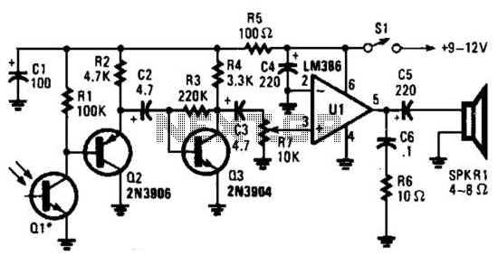
This receiver for amplitude-modulated light signals utilizes a phototransistor Q1 mounted within a parabolic reflector to enhance its range. Any NPN phototransistor is suitable for this application. An emitter-follower configuration using Q2 drives an amplifier stage Q3. The output...
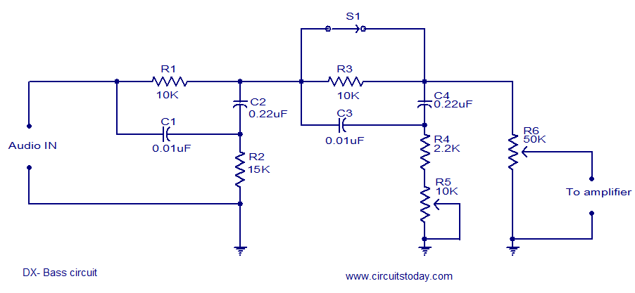
The circuit diagram of a passive DX bass circuit is presented, which is compatible with nearly all audio amplifiers. This design was created by Mr. Emmanuel Chipula from Malawi and submitted for publication. Laboratory tests confirmed satisfactory performance. Credit...
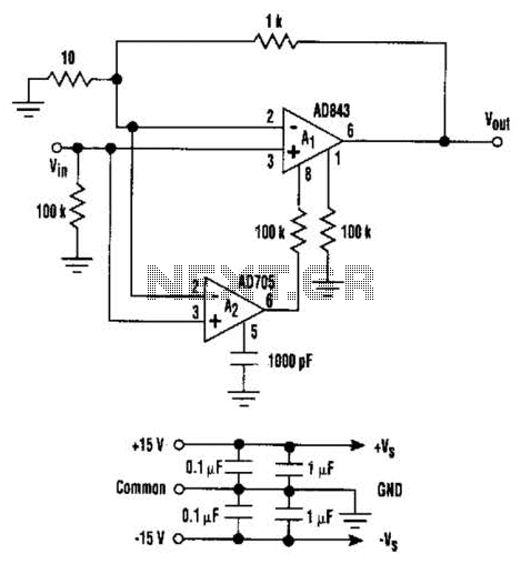
This circuit combines the advantages of low input offset voltage and drift without compromising the overall dynamic performance of the system. When compared to a standalone FET input operational amplifier, the composite amplifier circuit demonstrates a 20-fold improvement in...

The individual expressed frustration while attempting to connect a circuit to a 15V supply, bypassing resistor R3 with a clip-on soldering heat sink. They noted that 555 timers emit a distinct odor when damaged. They have limited components remaining...
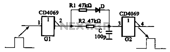
The inverter circuit using CD4069 is configured with a delay and width adjustment. When the output of the inverter (G1) is high, the capacitor (C) charges through resistor (R1) and diode (D). The voltage across capacitor C quickly reaches...
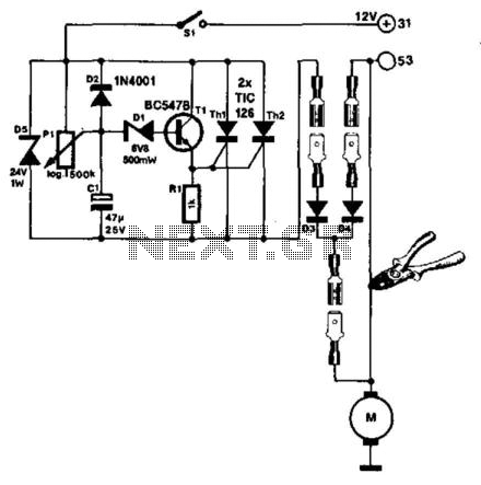
The windshield wiper interval circuit described here is compact and notable for utilizing two thyristors instead of a relay. It features only two connections and operates smoothly, even with multistage wiper circuits. The wire connecting the wiper motor to...
Warning: include(partials/cookie-banner.php): Failed to open stream: Permission denied in /var/www/html/nextgr/view-circuit.php on line 713
Warning: include(): Failed opening 'partials/cookie-banner.php' for inclusion (include_path='.:/usr/share/php') in /var/www/html/nextgr/view-circuit.php on line 713