
zener Floating Voltage to Bias a P-Channel Mosfet without Exceeding Source-Gate Max Voltage
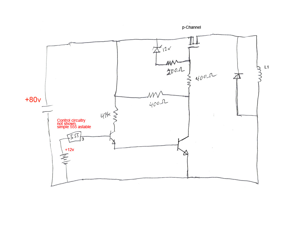
The circuit operates by utilizing a P-channel MOSFET to switch the current through the L1 coil, which generates magnetic fields when energized. The inclusion of a freewheeling diode is critical for safeguarding the MOSFET and other components from voltage spikes caused by the inductive load during the off state. The design incorporates a 555 timer configured in astable mode to generate the square pulse signal required to energize the coil. The output from the 555 timer is connected to the base of the BJTs, which act as switches to control the gate voltage of the P-channel MOSFET.
The resistor network plays a vital role in ensuring that the gate voltage is maintained at a safe level relative to the source voltage. This network is designed to deliver an adequate gate voltage that allows the MOSFET to switch effectively without exceeding its maximum gate-source voltage rating. The use of the 12-volt Zener diode is a protective measure that prevents the gate voltage from dropping too low, thus avoiding the risk of damaging the MOSFET. This diode will conduct when the gate voltage approaches 12 volts below the source voltage, thereby clamping the gate voltage and allowing for stable operation across a range of input voltages.
In summary, this circuit design effectively addresses the challenges associated with driving an inductive load using MOSFET technology while ensuring protection against back EMF and maintaining operational integrity across varying power supply conditions. Proper component selection and configuration are crucial for achieving the desired performance and reliability.The premise of the circuit is this: I want to power L1 coil with square pulses. You can see I`ve got a freewheeling diode to handle the back emf field collapse to protect the circuitry. From previous experiments and talking to others on here, I learned that using an N-channel mosfet on the high side of the coil like this doesn`t work because the large negative voltage during the back emf coil collapse puts negative voltage
on the mosfet source which causes the gate (at zero volts) to turn on while the field is collapsing. I experimented with BJTs and they make it easy to fix the problem, but they also get hot. I really want to use mosfets for the ability to pass a lot of current with minimal resistance. So I`ve switched to a P-channel mosfet in the circuit shown. This seems pretty simple but I`m adding a level of complexity. I want to have arbitrarily high voltage in the main circuit - 80volts shown here but it could be more or less. Since the voltage is prone to change in use conditions, the circuit design must be agnostic to the actual main power voltage.
In the 80 volt example shown, since the p-channel mosfet requires 80volts at the gate to turn it off, I have added a small resistor network to supply the required voltage from the power src. You can see I`m using a 555 and some BJT`s to pull down the gate voltage to turn it on. Now the tricky part. From my understanding, I can`t drop the mosfet gate all the way to 0V because that would make an 80volt difference between the Source and the Gate which would destroy it.
I need to make sure the gate drops to about 12 volts less than the Source but drops no further. THe solution I`ve come up with is to add a 12 volt zener diode and adjust the resistances accordingly so once the gate starts to become more than 12 volts less than the source, the diode will reverse bias and bring the gate back up. It should stay right around 68volts if the power supply is 80 volts - as long as the BJT is biased on anyway.
Once the BJT turns off, the gate will recover to 80 volts and shut off the mosfet. 🔗 External reference
Related Circuits

This circuit illustrates a remote control circuit diagram using RF technology without the use of a microcontroller. Features include a simple remote control circuit that operates via radio frequency. The remote control circuit operates by transmitting signals through radio waves,...
Field bus technology and intelligent instrument technology are currently two of the most rapidly evolving technologies in automation and control. In the realm of field bus technology, the CAN bus has established itself as a relatively fast communication standard...
R1_47K 1/4W Resistor, R2_4K7 1/4W Resistor, R3_22K 1/4W Resistor, R4_1K 1/4W Resistor, R5, R12, R13_330R 1/4W Resistors, R6_1K5 1/4W Resistor, R7_15K 1/4W Resistor, R8_33K 1/4W Resistor, R9_150K 1/4W Resistor, R10_500R 1/2W Trimmer Cermet, R11_39R 1/4W Resistor, R14, R15_R33 2.5W...
The title of this article raises the question of why the extensive selection of fully integrated voltage regulators should be supplemented with a version built using discrete components. Specifically, what advantages does this circuit provide that the well-known three-terminal...
A regulated and noise-free power supply voltage is essential for microcontrollers and other components such as amplifiers, filters, and GPS devices. Voltage surges in the supply voltage can permanently damage embedded systems. A voltage regulator must maintain the output...
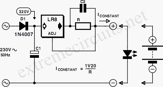
Commonly used 3-pin linear voltage regulators, such as the LM317, typically cannot handle input voltages exceeding approximately 30V. The LR8A from Supertex Inc is a new adjustable three-pin regulator that can accept input voltages up to 450V and can...