
Clock synchronization oscillator circuit
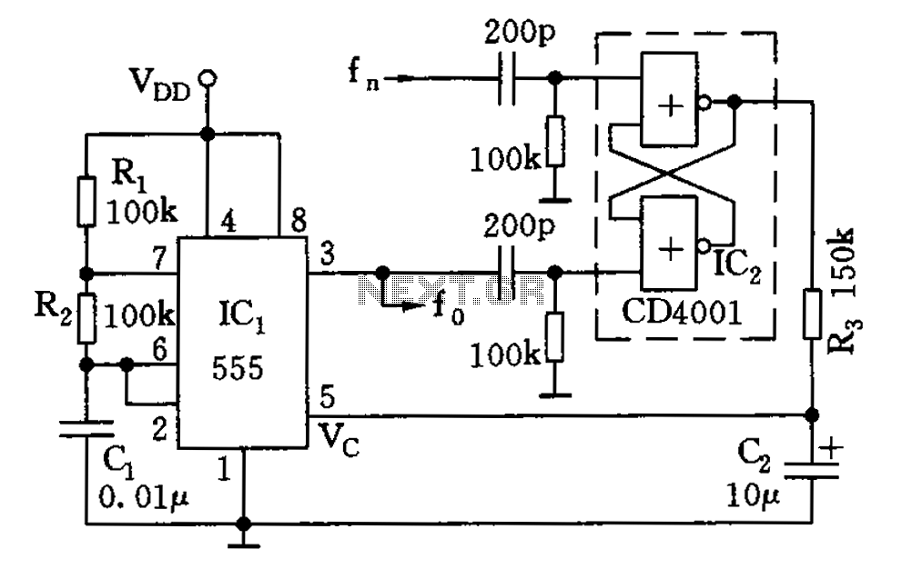
The circuit described employs a 555 timer configured in astable mode, which generates a continuous square wave output. The frequency of oscillation is determined by the values of resistors R1 and R2, as well as capacitor C1, following the standard formula for a 555 timer in astable operation:
\[ f_o = \frac{1.44}{(R1 + 2R2) \cdot C1} \]
The control terminal, often labeled as pin 5 on the 555 timer, can be used to adjust the DC level of the output frequency. This adjustment allows for fine-tuning the oscillation frequency, enhancing the versatility of the circuit.
The output from the 555 timer is fed into an RS flip-flop, implemented using two NOR gates from the CD4001 IC. The RS flip-flop serves to lock the output signal, ensuring a stable duty cycle. The duty cycle is defined as the ratio of the time the output is high to the total period of the waveform. When the circuit is in a locked state, the duty cycle remains unchanged, which stabilizes the DC level produced by the low-pass filter.
The low-pass filter is crucial as it smooths out the square wave output from the RS flip-flop, providing a more stable DC voltage. The relationship between the oscillation frequency and the DC control level is significant; as the frequency increases, the duty cycle also increases, which in turn raises the DC level. Conversely, a decrease in frequency results in a lower duty cycle and a corresponding decrease in the DC level. This dynamic interaction between frequency, duty cycle, and DC control level is essential for applications requiring precise timing and control in electronic circuits.
Overall, this circuit design showcases the integration of a 555 timer, RS flip-flop, and low-pass filtering to achieve a stable multivibrator output, making it suitable for various timing and control applications in electronics.As illustrated, 555 and R1, R2, C1 composition controlled multivibrator, its oscillation frequency in addition to the RC time constant related to, but also by the control termi nal of the DC level is adjusted. While the DC level from the reference frequency f. 555 output and the oscillation frequency fo Nfn common locking square wave output of RS flip-flop, after the low-pass filtered to produce. CD4001 two NOR gates as RS flip-flop, RS flip-flop in the locked case, the duty cycle of the output unchanged, thus filtered DC level unchanged.
If the oscillation frequency f0 of 555 to a high drift (or fn fall), the duty increase, DC control level will be a corresponding increase in frequency will decline; and vice versa.
Related Circuits
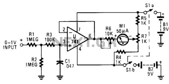
The circuit is designed around a 741 general-purpose operational amplifier (op amp) configured as a voltage follower, providing a voltage gain of one. The output from the 741 is utilized to drive a 50-meter movement. Potentiometer R7 is employed...
This project was a surprise as the BC547 transistor (equivalent to 2N2222) can be used to construct a 500mW linear amplifier that operates across the entire HF band with excellent spectral purity and without the need for neutralization. The...
The ability amplifier has remained functional since it was first introduced in 2002. It is not broken, so there is no reason to fix it. The accompanying photo shows a well-assembled board (known as M27). Utilizing TIP35/36C transistors, the...
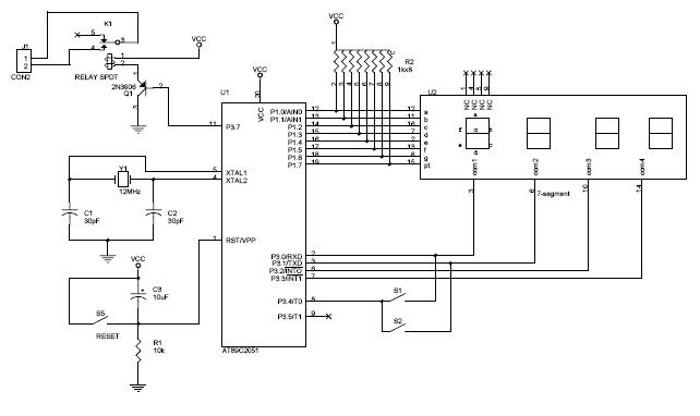
The circuit diagram above illustrates the Clock Controller V1.1. Pins P3.0 to P3.3 are connected to the base of a 4-PNP transistor, specifically the 2N2907, which is used to sink current. The Clock Controller V1.1 circuit is designed to manage...
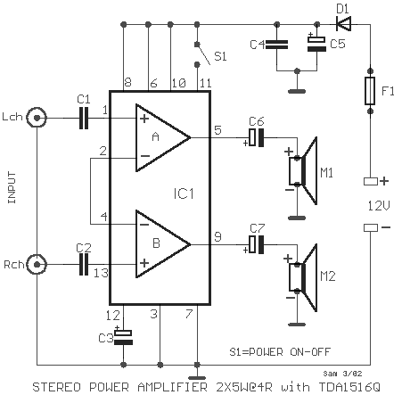
A simple stereo amplifier with minimal external components. It utilizes only one operational amplifier, which is capable of delivering an output power of 2x5W into a 4-ohm load, with a distortion of 0.5%. This stereo amplifier circuit is designed to...
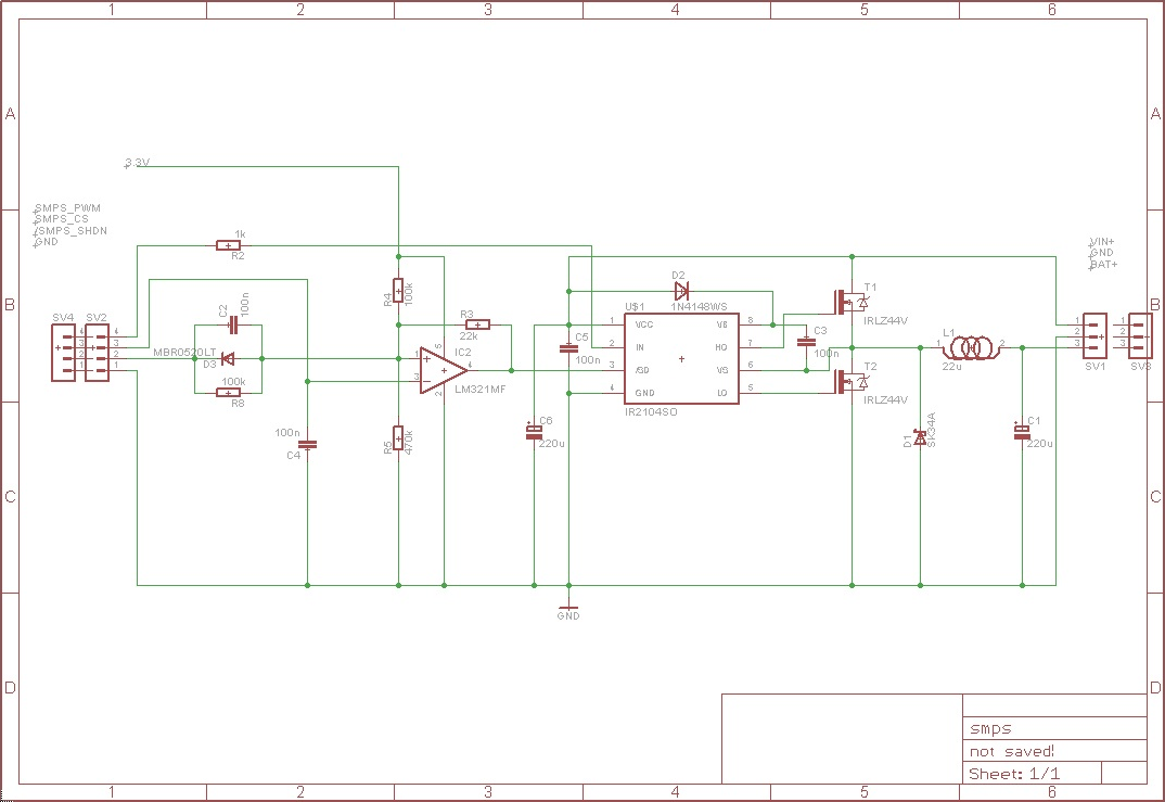
The circuit receives an input voltage (Vin), which is processed through a Switch Mode Power Supply (SMPS) utilizing two MOSFETs driven by an IR2104 driver. The output is directed to the battery positive terminal (Bat+). An LM321 operates as...
Warning: include(partials/cookie-banner.php): Failed to open stream: Permission denied in /var/www/html/nextgr/view-circuit.php on line 713
Warning: include(): Failed opening 'partials/cookie-banner.php' for inclusion (include_path='.:/usr/share/php') in /var/www/html/nextgr/view-circuit.php on line 713