
As of control rechargeable delay circuit

The control rechargeable delay circuit operates effectively by utilizing two transistors, VTi and VTz, to manage the signal input and output states. In the absence of an input signal, VTi remains in the off state, allowing VTz to conduct. This configuration ensures that the output voltage (U) is maintained at a low level, effectively grounding the output.
Upon receiving an input signal, VTi switches to the on state, which simultaneously turns off VTz. This transition causes the output voltage (Us) to rise to a high potential, indicating the presence of the input signal. The circuit's behavior is governed by the timing characteristics defined by the RC time constant, which is influenced by the resistive (R) and capacitive (C) components within the circuit.
The delay period during which the output remains high after the input signal is removed is determined by the equation t = RC ln(Vs/V). This relationship illustrates how the time delay is affected by the ratio of the regulator voltage (Vs) to the voltage across the components (V). The stability of the time characteristics is enhanced when the condition UMW/E = -0.37 is met, leading to a more predictable and reliable output response.
In practical applications, this delay circuit can be employed in various electronic systems where timed responses to input signals are critical. Its design allows for flexibility in adjusting the timing characteristics through the selection of appropriate resistor and capacitor values, enabling it to meet specific operational requirements in control systems, timers, and other electronic devices.As of control rechargeable delay circuit Under normal circumstances, when there is no input signal, the transistor VTi off. VTz conduction, the output U. Low potential. When U. , So that the signal voltage VTi turned, VTz off, the output Us. High potential. When Ua, signal disappears, VTi off, VTZ conduction, U.. He reverted to the low potential. From U. The signal appears to U ;. It goes high for the time interval delay circuit at the time. can be calculated as follows: z RCln poison (s) where U MN- regulator vs becomes turned off by the M, the voltage between N, V. When UMW/E. -0. 37 when, t-RC, time characteristics more stable, and can be the most time-lapse t...
Related Circuits

In applications where a MOSFET is employed to switch a load, incorporating short-circuit or overload protection is straightforward. This can be achieved by utilizing the internal resistance RDS(ON) of the MOSFET, which generates a voltage drop proportional to the...

Figure 1 consists of a Programmable Unijunction Transistor (PUT) and an automatic interval timer circuit. In this circuit, the PUT serves as the oscillator. The switch S1 is used to toggle between interval timing and automatic timing modes. When...
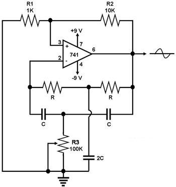
This circuit generates a sine wave using a single operational amplifier (741). The feedback loop of the op-amp includes a twin-T filter connected between its output and inverting input. Positive feedback for oscillation is provided by resistor R2. The...
An oscillator circuit of this nature is often utilized as a clock circuit. This circuit employs a crystal frequency control with a stability of one million hertz. An oscillator circuit designed for clock applications typically generates a periodic signal, which...
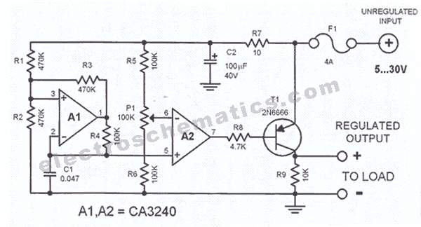
This circuit regulates a DC power output and has a wide range of applications. It can be utilized to control the speed of a motor, a pump, a toy train, or the brightness of an LED or lamp. Essentially,...

Power Amplifier Speaker Protection Circuit Schematic. When a power amplifier is switched on, a loud thump sound is often heard due to a sudden heavy discharge. The power amplifier speaker protection circuit is designed to prevent loud thump sounds during...