
Units from the MAX4100 4101 gain buffer circuit diagram

The MAX4100/4101 unit gain buffer circuit is designed to provide high-speed signal buffering with minimal distortion. The operational amplifiers in this configuration are known for their low input offset voltage and high slew rate, making them suitable for applications requiring fast response times. The inclusion of a 24-ohm feedback resistor is a strategic choice; it balances the need for stability against the potential for increased noise and distortion.
In this circuit, the feedback resistor serves multiple purposes. Primarily, it helps to control the gain of the amplifier, ensuring that the output remains a faithful reproduction of the input signal without amplification or attenuation. This is crucial in applications such as signal conditioning, where preserving the integrity of the signal is paramount.
Moreover, the resistor's presence in the feedback loop aids in dampening oscillations that may arise from the inherent capacitance and inductance present in the circuit. By providing a controlled path for feedback, the resistor stabilizes the operational amplifier's response, allowing for a fast settling time that is essential in high-speed applications.
The characteristics of the MAX4100/4101 make them ideal for use in a variety of electronic applications, including audio processing, sensor signal buffering, and data acquisition systems. The unit gain buffer configuration ensures that the circuit can drive capacitive loads effectively, making it suitable for interfacing with other stages of a signal processing chain without introducing significant phase shifts or delays.
Overall, this unit gain buffer circuit exemplifies effective design principles in electronic engineering, focusing on stability, speed, and signal integrity, which are critical for modern high-performance electronics. As shown by FIG MAX4100/4101 unit gain buffer circuit constituted. This circuit uses a small resistor (24 ) placed in the feedback loop amplifier constituting a unity gain buff er, so the maximum bandwidth of the circuit, and has a low overshoot and fast settling time; at the same time this resistance can inhibit parasitic inductance and capacitance of the negative influence the stability of the circuit best, it can also reduce the error caused by the input bias current. VOUT VIN.
Related Circuits
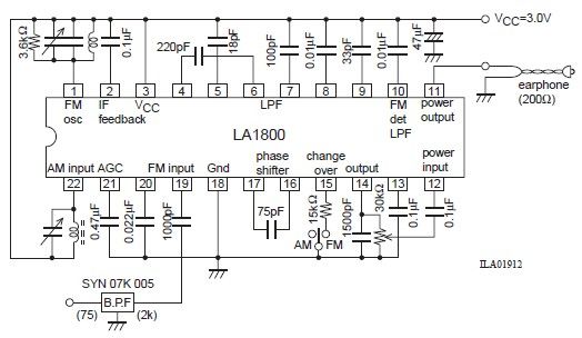
This portable AM/FM radio circuit is designed using the LA1800 integrated circuit (IC) along with several external components. The LA1800, manufactured by Sanyo Semiconductors, requires only a few additional components for its operation. The output signal is directed to...

The automotive LED driver circuit diagram utilizes the LT3486. The LED is employed in the car's central high-mounted stop lamp (CHMSL), providing advantages such as faster achievement of the set brightness, higher efficiency, longer lifespan, and simplified design and...
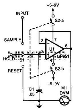
This circuit demonstrates the principle of the sample-and-hold circuit. SI can be replaced by electronic switches (FET, etc.) in an actual application. The sample-and-hold circuit is an essential component in various analog-to-digital conversion applications. Its primary function is to capture...
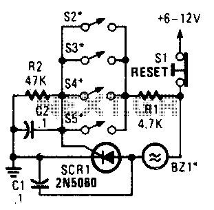
Four parallel switches are employed to monitor four positions. When any switch is closed, SCR1 is triggered, activating the alarm. The alarm is designed to be of the non-interrupting type. The circuit consists of four parallel switches, each representing a...

This DIY sound-activated lights circuit turns a lamp on for a brief duration when a dog barks or when a relatively loud sound is detected, creating the impression that the occupants are alerted. The condenser microphone is positioned to...
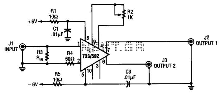
This circuit selects one of two channels using a logic signal. The unused channel is shorted out to minimize crosstalk. The bandwidth at -3 dB is approximately 8 MHz. It is recommended to buffer this circuit due to some...